The fast buses on the SDS7102
This is a post in a series about me poking at the insides of my OWON SDS7012 oscilloscope. You might want to start reading at the beginning.
As you might recall there is one very important bus in the scope that connects the SoC to the FPGA. The FPGA is supposed to emulate a DDR2 memory connected in parallel with the real DDR2 memory to the SoC. This is a fairly fast bus running at 133MHz with data being transferred on both edges of the clock.
“How hard can it be anyway?”
The thing that makes a DDR bus a bit tricky is is that it actually works in multiple different clock domains at the same time. For a 16 bit DDR bus there are three clock domains, one for the control signals, and one for each of the 2 bytes of data. For a 32 bit DDR bus there are five clock domains, control + 4 bytes of data.
The DDR controller control signals are always driven by the SoC and are synchronous to the DDR clock. These are the chip select (/CS), row address select (/RAS), column address select (/CAS), write enable (/WE), bank address (BA[1:0]) and address (BA[11:0]) signals. These signals are single data rate (SDR) which means that they should be sampled on the positive edge of the DDR clock.
Data is transferred on the DQ signals using the DQS signals as a clock. Data is transferred at double data rate (DDR), that is, on both the positive and negative edge of the DQ signal. Each byte worth of DQ signals has its own DQS signal. The DQS clock should be running at the same frequency as the DDR clock but can vary slightly and can also be slightly off in timing for each byte.
The reason each byte worth of DQ signal has its own DQS signal is that many DDR DIMMs are built using DDR chips that only have an 8 bit wide bus. Each chip has its own timing and own DQS signal.
For writes there are is a /DM signal present for each byte. A low on /DM indicates that the byte contains data that should be written to memory, a high on /DM indicates that no write should be performed. The timing for the /DM signal is the same as for the DQ signal.
Someone who wants to implement a 16 bit DDR memory properly has to do something like this:
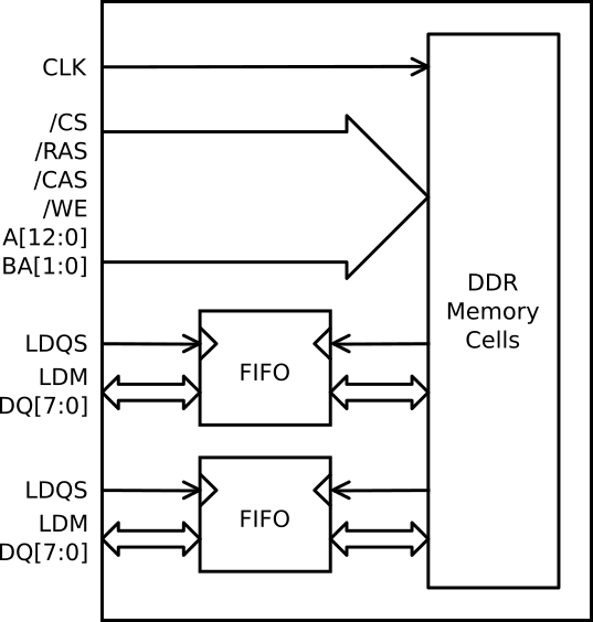
Each byte worth of data needs its own FIFO which is clocked by the DQS signal. LDQS is the lower data strobe for the low byte, UDQS is the upper data strobe for the upper byte. Not that easy to get right.
Read only DDR memory
Then I realised that the bulk of all data transfers are going to be sample data from the FPGA to the SoC. For the few transfers I have to do from the SoC to the FPGA I can use the slow SPI bus I already have and have been using for a while. So I can get away with emulating a read only DDR memory, and in that case I can transfer all data using the DDR clock and don’t have to care about multiple clock domains.
That would make everything much easier, all I have to do then is to figure out how to use the ODDR2 primitives of the Xilinx FPGA to be able to transfer data using DDR on both edges of the clock.
I could even use a read from a specific address to tell the FPGA that I have finished reading data and that it can perform a new capture.
I could probably manage that.
DDR Protocol
Since there can be multiple DDR memory chips connected to the same DDR bus each memory has a separate chip select (/CS). When /CS is low the chip is selected.
To access a DDR memory a bank must be opened and a row selected. This is done by sending a Bank Activate command which is performed when /CS
- /RAS are low and /CAS + /WE are high, with the bank and row addresses present on BA and A.
The controller can then perform multiple reads or writes to the active bank and row. A read command is performed when /CS + /CAS are low and /RAS + /WE are high. Data is transferred a few cycles later on the DQ lines (with DM as a data mask on writes) using DQS as a strobe. Data is always transferred in bursts. For the DDR memory in the SDS7102 a burst consists of 4 words. If the DDR controller wants to read a single word it transfers all 4 words in the burst but can throw away the 3 words it doesn’t need.
A write command looks almost identical to a read except that /WE is low. The /DM signals which are transferred in parallel to the DQ signals are used to specify which words of a burst should be written to memory.
Its possible to perform multiple read and write commands to the same row. One bank select command could be followed by a read command and then a write command.
There are a few more commands in the DDR protocol. There are configuration commands which configure parameters such as the burst length and the CAS latency - the time from the read/write command until the data transfer starts. Other commands perform a refresh of a bank or put the memory in power saving mode. After a bank has been opened it must be precharged using yet another special command before it can be accessed again. As an optimization the last read/write command can hold A10 high indicating that the memory should perform an automatic precharge of the bank.
Implementation
I wrote myself a DDR controller that simulated beautifully. It doesn’t really do anything, all it does is return the address of each word as the data. I start reading a burst of 4 16-bit words starting at 0x20 I should get the following results back:
0x0020 -> 0x0020
0x0021 -> 0x0021
0x0022 -> 0x0022
0x0023 -> 0x0023
But of course didn’t work at all when I tried it in the FPGA. To speed things up I tried to use the control signals (CS, RAS, CAS, WE) directly in my test for a read operation:
if not bus.CS_B and bus.RAS_B and not bus.CAS and not bus.WE:
    rd_active.next = 1
That it didn’t work is not too surprising, if the time from when the control signals change until the positive clock edge when I use the result is too short the combinatoric logic will not have time to settle and I will get invalid results.
With an external bus the right thing to do is to immediately store the external values in internal registers and only use the registered values. This aligns the values to the internal clock and gives the combinatoric logic a full clock cycle to settle.
Unfortunately, this increases the delay before the FPGA returns the results to the SoC. I would see garbage in the first odd words and after that I would see data that should have been returned by previous reads:
0x0020 -> 0x0020
0x0021 -> 0x3800
0x0022 -> 0x0022
0x0023 -> 0xe284
0x0024 -> 0x0024
0x0025 -> 0x0021
0x0026 -> 0x0026
0x0027 -> 0x0023
Huh? How can this happen?
But it actually makes sense. The DDR controller has two receive FIFOs for each byte, one FIFO which stores data from the positive edge of DQS and a second FIFO which stores data from the negative edge of DQS. When the DDR controller expects the transfer to finish it reads out the data from the FIFO. If my emulated DDR memory is too slow the last falling edge of DQS will be too late and reading from the negative edge FIFO will return strange data.
I finally realised that I was wasting one clock cycle in my DDR code which I could remove. This means that could start the data transfer earlier and the last negative clock edge would not be too late and data started showing up as it should on the SoC.
I did have occasional problems with corrupted bits and I thought this might be due to the DQS signal arriving too early at the SOC so I added some Xilinx IODELAY2 primitives to delay the DQS signals slightly and that seems to have helped.
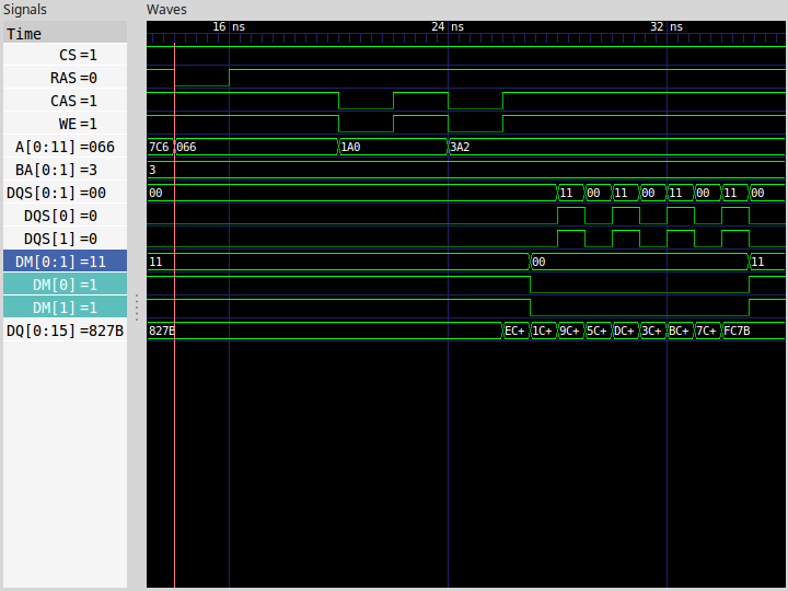
Here’s how a burst read from the FPGA looks for real:
I’m not sure if I have implemented all this correctly, but it does seem to work in practice, so I’ll just nod and be happy.
The other fast bus
The other fast bus in the scope is the memory bus between the FPGA and its own DDR memory. This also worried me because OWON ignored the Xilinx requirement that “RZQ is not optional”.
Well, I finally tried. I used the Xilinx core generator tool to create a memory controller which I then added some glue code for in MyHDL. I did not connect the RZQ line which stopped the memory controller from synthesizing. But after reading the generated verilog code a bit I found a parameter in the memory controller “C3_CALIB_SOFT_IP” that I could set to “FALSE” which stopped it from trying to use the RZQ line and that gave me a .bin file that I could load into FPGA.
I did, and as far as I can tell the DDR controller is actually working. The “calib_done” line is high indicating that the DDR controller managed to calibrate itself and the error line from the test bench is low indicating that it hasn’t seen any errors so far. I first ran the memory controller at 133Hz, but then raised the clock frequency to 266MHz and finally 333MHz. I also tried 400MHz but then the error flag went on indicating that something was wrong.
Even so, at 333MHz the DDR controller should be able to transfer 333 * 2 * 2 = 1333 MBytes per second during a burst. There’s a fair bit of overhead between each burst but this should still be enough to be able to store 1Gsample/second from the ADC into DDR memory with a bit of bandwidth to spare.
So if the DDR controller is actually working, and I haven’t messed up my calculations of the clock speed, and the DDR controller will be stable at this speed, and there’s nothing else wrong, it seems that I should actually be able to use both the fast bus to the SoC and the DDR memory.
Now I just need to tie all this together.
Everything I’ve written about here is available in my SDS7102 repository on GitHub. Note that I’ve switched to newer versions of both Buildroot and the Linux kernel. Take a look at README.md and run “./update.sh” if you are using an older version from my repository. And run “git log –stat” to see which checkins do what and what files they affect.
Update: A new post here.