Hacking the OWON SDS7102 Scope
A few years ago I bought myself an OWON SDS7102 oscilloscope.
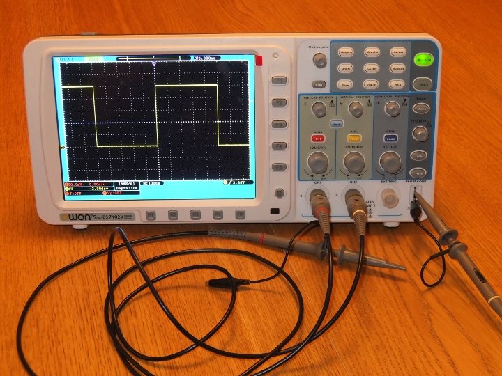
The specifications for the scope are rather nice: decent bandwidth and sampling rates, a large bright display, a battery option and lots of connectivity such as a USB host, USB device and Ethernet. The scope is pretty crappy in some ways though. The analog section is fairly noisy so don’t expect to see any details for signals below 1mV at X10 attenuation. The firmware is a bit buggy and some things just don’t work. Trying to save images to a USB memory hangs until the USB memory is unplugged. Trying to talk to the scope over ethernet crashes the scope. The menu system is a bit messy.
(I know, the reason the USB memories won’t work is that the sector size is wrong. I’d still consider that a big wart since there are no error messages and this information isn’t that easy to find.)
Still, it has been very useful. I have a much fancier, and of course much more expensive, Hameg scope at the office. The Hameg has a better analog section, the noise is noticeably lower than with the OWON, it has a higher sampling rate, can decode a bunch of different protocols, has a logic analyzer, and has more math functions than I can shake a soldering iron at and is just better in so many ways. It’s a solid piece of German engineering. But engineers aren’t always that good at user interfaces so it’s also a bit clunky to use.
Usually when I need an oscilloscope it’s because I’m looking at something like an I2C bus or a SPI bus and for that it doesn’t really matter if the measurements are a bit noisy down a 10mV and I don’t need that high sampling rates. The large display and the fact that the all the knobs and buttons are in the natural places makes the OWON really nice to use. The OWON also fits perfectly in an old laptop bag I have, and since it cheap enough that I’m not too worried about breaking when I’m carrying it around. If I were to break it I can afford a new one. Being able to run the scope off the battery is also a real plus in some situations. Despite all its fault the OWON has somehow ended up being up the scope I use most of the time.
The “hacking” part
One of the reasons I bought this specific scope was that I had seen some teardowns of it and knew that the scope has a Samsung System-on-Chip (SoC) and a Spartan 6 FPGA in it and I have some familiarity with both. At the back of my head I had the idea that I might be able to reverse engineer the scope and do something interesting with it.
Two years after buying the scope I still hadn’t done anything like that with it though. But about a week ago I finally decided to do something.
A word of warning here. This is probably going to be yet another project where I start, spend some time on it and then lose interest, so there’s a big risk that I won’t reach my goal. But the road there might be interesting anyway.
What is reverse engineering?
Figuring out how something like this works is called “reverse engineering”, the idea is that you are looking at a finished product that someone has build and you are trying to reverse the engineering process that went into designing the thing.
There is a huge thread discussing the SDS7102 on EEVblog forums and other people has done quite a bit of reverse engineering of it already. They have mostly concentrated on the analog parts and I’m more interested in the digital parts and the firmware.
Disassembling the scope
Where to start? The first thing to do is usually to open up the thing you’re interested in and try to identify the main components. I opened up my scope and started removing parts until I found the main board which contains all the smarts.
The next step was to try to identify the main components on the board and get a general feel for how they work together.
Components on the front
This is the side of the main board that’s facing the front of the scope.
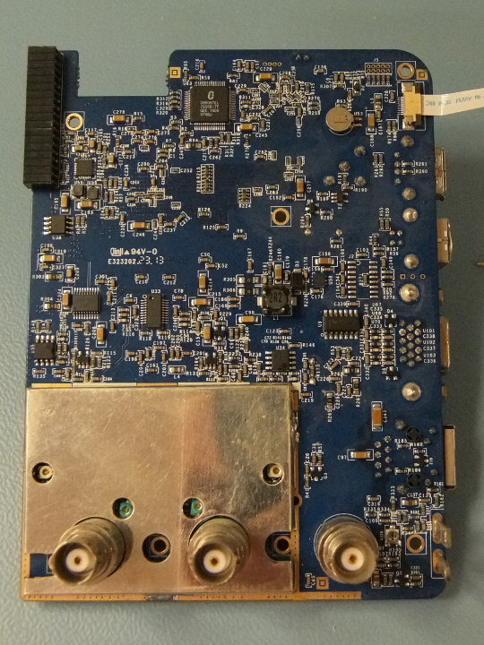
The connector to the LCD board is in the upper left corner and the connector to a separate board with all the knobs and buttons is in the top right corner. The square component at the top has “Chrontel 7026B-TF” printed on it and a quick internet search confirms that it is a “7026B TV/VGA Encoder” from the company Chrontel. Other than that there’s not much interesting to see here. All the good stuff of the analog frontend (AFE) is hidden beneath a shield that I would prefer to not remove if I can avoid it. Someone called “tinhead” on the EEVblog forums has already reverse engineered the AFE so hopefully I won’t have to do it.
Components on the back
I’m more interested in the digital parts and the back of the main board has a lot more of that.
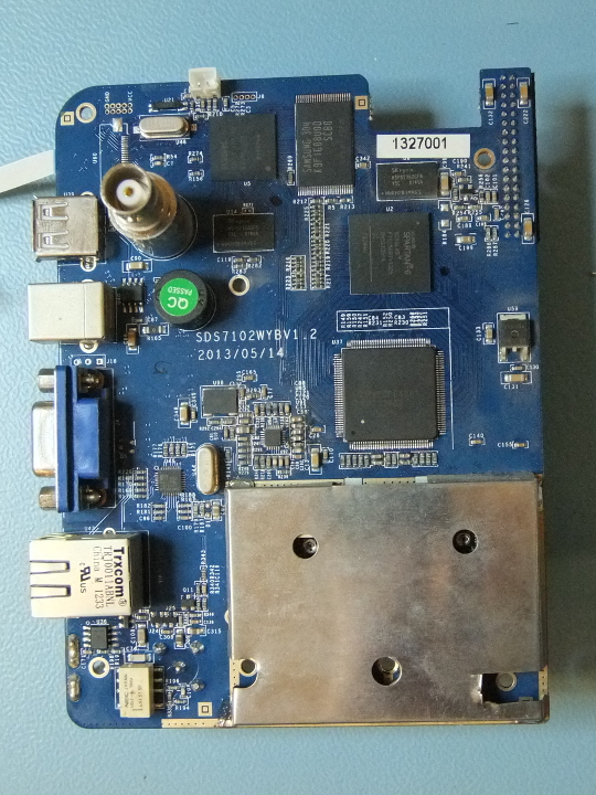
The square component at the top is the Samsung S3C2416 SoC. To the left of the CPU is metal can which has 12.0000M printed on it. A metal can like this is almost always a crystal, so it ought to be the main 12MHz crystal for the SoC. The component to the right of the SoC has Samsung K9F1G08U0C printed on it and and quick internet search tells me this is a 128Mx8bit NAND flash memory. From the traces that are visible on the PCB it looks like it’s connected to the SoC, and this makes sense too since the SoC will need something to load its firmware from. The component below the SoC is a Hynix H5PS5162GFR 64Mx16bit DDR2 memory and the traces also go to the SoC. This also makes sense since the CPU needs memory to run the firmware in. So far so good.
Correction: it’s a 32Mx16bit or 64MByte DDR2 memory.
The chip below and right of the SoC is the Xilinx Spartan 6 XC6SLX9 FPGA. The component above the FPGA turns out to be one more Hynix DDR2 memory. From looking at the traces that are visible on the PCB it seems to be connected to the FPGA so this is probably used for the waveform storage. The FPGA has a lot of traces to the big component below it which has a National Semiconductor logo and “VE206ABE3” and “S7002952”. A search on these two doesn’t show up anything, but after digging a bit more it turns out that it ought to be an ADC08D500 8 bit A/D-converter (ADC) which can sample two channels at 500Msamples/second or one channel at 1Gsamples/second. This matches the specifications for the scope and also makes sense. Two differential pairs of traces sneak down below the shield and ought to be ADC inputs from the AFE.
To the left of the the ADC is a component marked ADF and 4360-7, it’s an Analog Devices ADF4370-7 “350 to 1800MHz Integrated synthesizer and VCO”. The component above and to the left of is marked with “0.100000” and “DCP1311 1315”. I haven’t been able to find any more information about it, but I would guess that it’s a crystal oscillator of some kind which is used as a reference for the ADF4360 clock synthesizer.
Close to the ethernet connector there’s a Micrel KSZ8851 Single port Ethernet MAC/PHY. Next to it is a metal can which is marked L25.000M and there are two traces from the can to the oscillator pins of the KSZ8851. 25MHz is a very common frequency used for ethernet chips so it’s obviously the crystal for the it.
Finally there’s a component marked AT88SC 0401CA which I couldn’t find a perfect match for. It is probably an Atmel “CryptoMemory”-something which is probably used for copy protection, some way of storing and verifying the serial number of the unit.
Pin headers
The most interesting thing isn’t any of the components though. It is what isn’t mounted on the PCB. Quite often parts that haven’t been mounted are things that are used during software development but aren’t needed when the units are mass produced such as connectors for a serial port for debug messages or a JTAG programmer which can be used to load and debug software.
Above the Samsung SoC there are four holes for a pin header which could a serial port. In the top left corner there are ten more pins for a pin header which is probably for a JTAG programmer. There are another three holes between the VGA and USB B connector which could be yet another serial port.
Summary
It was time to call it a day. I have identified the most important components on the main board and have a pretty decent idea of how they are connected. The empty pin headers might give me access to a bootloader or allow me to connect a JTAG programmer so that I can look at the existing firmware or load my own firmware into the SoC.
What is nice is that a lot things in the scope such as DDR memory, NAND flash, LCD, USB host, USB device and serial ports are connected to interfaces that are built into the SoC; there aren’t that many ways that they can be wired up. The connections between the SoC and the DDR memory or the NAND flash must be made in a specific way, otherwise they won’t work at all. This means that it ought to be fairly easy to make them work.
The ethernet controller is an external component, but the pins of the IC are exposed so it should be fairly easy to probe them and figure out how they are connected to the SoC. The thing that worries me is that both the SoC and the FPGA and the DDR memory connected to the FPGA are all BGA packages with no exposed pins; figuring out the connections between them might be impossible.
It’s hard to know when to quit
Before packing up I just had to try something first. I tried probing the four pins above the SoC. No luck, they don’t seem to do anything.
I had more success with the three holes next to the VGA port. The center pin turned out to be ground and the other pins are transmit and receive of a serial port.
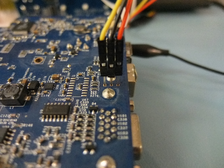
When I connected a USB-serial adapter those pins, set my terminal program to 115200 bps and powered on the oscilloscope I got the following output:
******************************
LILLIPUT
DSO TARGEY BOARD VER 1.0
LILLIPUT

SamSung MCU S3C2440
Program Ver 1.0(2006613)
 FCLK = 400000000Hz,  USB Crystal Type : 12M
****************************
*          LOADBOOT        *
*                          *
*          LILLIPUT        *
*           (2004)         *
****************************
Boot to load (Y/N)?
Wait for Enter . . . . . . . . . . . . . . . . . . . . . . . . . . . . . .
DSO TARGEY BOARD VER 1.0
Lilliput is the company that owns the OWON brand.
Neat, that’s something to play around with the next time.
Update: This series is continued here.