Hacking the OWON SDS7102 Scope (Part 2)
In my previous post I had disassembled my OWON SDS7102 scope and had just been able to locate a debug serial port where I could see some messages from a bootloader.
******************************
LILLIPUT
DSO TARGEY BOARD VER 1.0
LILLIPUT

SamSung MCU S3C2440
Program Ver 1.0(2006613)
 FCLK = 400000000Hz,  USB Crystal Type : 12M
****************************
*          LOADBOOT        *
*                          *
*          LILLIPUT        *
*           (2004)         *
****************************
Boot to load (Y/N)?
Wait for Enter . . . . . . . . . . . . . . . . . . . . . . . . . . . . . .
DSO TARGEY BOARD VER 1.0
That looked very promising. But nothing happened when i pressed Y or Enter, the bootloader would just continue and load the oscilloscope firmware. I finally gave up on the serial port and started looking for a JTAG port.
I later disassembled the bootloader and discovered that it listens for the character “u” and this makes the bootloader stop and wait for a connection over USB. As far as I can tell there are no other characters or magic phrases that makes it do something else. I did find code in the disassembly for some kind of command prompt but I haven’t figured out how to access it. The command prompt might have been disabled permanently even though there are traces left of it in the code.
JTAG
JTAG is an acronym for Joint Test Action Group which was originally a standard for testing assembled PCB. Using something called Boundary Scan it is possible to control all the I/O pins of an IC and this can be used to to verify that all the pins of an IC are connected correctly. For ICs with a built in processor, such as the ARM CPU in the Samsung S3C2416, it can provide a debug interface to the procesor.
The mandatory pins for a JTAG port are Test Clock (TCK), Test Mode Select (TMS), Test Data In (TDI), and Test Data Out (TDO). Optional pins are Test Reset (TRST) which is used to reset the JTAG interface itself or System Reset (SRST) which is the reset for the whole system. It’s also good practice to have a voltage reference (VREF) pin with the voltage that should be used to drive all the other pins. It’s of course also necessary to have a ground (GND) pin.
This makes about half a dozen pins but they can be arranged in many different ways. Sometimes a PCB doesn’t even even have a JTAG connector, the JTAG pins can be spread out over the PCB or only accessible as test points or at a component pad. Sometimes JTAG is hidden, either by covering it with a sticker or by having JTAG on a piece of the PCB that is broken off from the main PCB after manufacturing.
There was space on the SDS7102 for a 2mm 2x5 connector that looked very promising though. Probing it with a multimeter showed that the five pins on one side were all connected to VCC or GND and the other pins were connected to a couple of resistors. If this was a JTAG port four of the pins on the other side would be the mandatory pins and the fifth probably a reset or not connected at all. There is a list of JTAG connector pinouts but it only contains a fraction of all possible and used pinouts. And unfortunately none of the connector pinouts matched the one I’d found.
There is an interesting project called JTAGulator which uses a custom built piece of hardware to test all pin combinations by brute force. There are also some interesting slides and videos on that page with more details on how to discover JTAG interfaces in a device. I didn’t have to do any of this though. That “tinhead” had already figured out the pinout and posted about it on the EEVblog forums.
The pinout of the connector is:
RST 1    2  GND
TMS 3    4  GND
TDO 5    6  GND
TDI 7    8  VCC
TCK 9   10  VCC
I soldered some wires to both the JTAG port and the serial port. I then put the scope back together with the wires sticking out on the side:
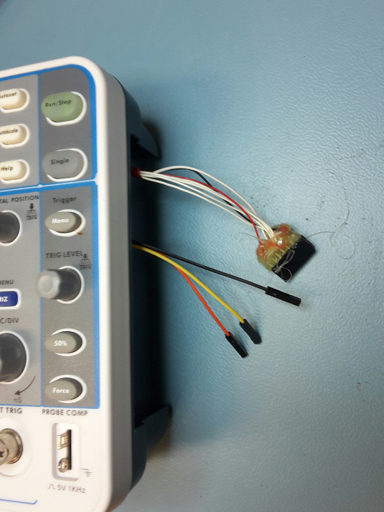
The three loose wires are transmit, receive and ground from the serial port. The big connector is compatible with a Bus Blaster MIPS that I had lying around.
OpenOCD
OpenOCD is a tool to use a JTAG adapter totalk to a debug interface on a chip. Among other things it has support for the Bus Blaster as a JTAG debug adapter. It does not have support for the S3C2416 specifically, but it does have support for some other SoCs in the Samsung S3C family and they ought to be fairly similar.
The documentation for OpenOCD is not all that good, but after a lot of trial and error I had managed to piece together an “openocd.cfg” which looks like this:
source [find interface/ftdi/dp_busblaster.cfg]
adapter_khz 1000
reset_config srst_only srst_open_drain
reset_config trst_and_srst

jtag newtap s3c2416 cpu -irlen 4 -ircapture 0x1 -irmask 0xf -expected-id 0x07926f0f

target create s3c2416.cpu arm920t -endian little -chain-position s3c2416.cpu
Running OpenOCD shows that it found something:
$ openocd -f openocd.cfg
...
Info : clock speed 1000 kHz
Info : JTAG tap: s3c2416.cpu tap/device found: 0x07926f0f (mfg: 0x787 (<unknown>), part: 0x7926, ver: 0x0)
Info : Embedded ICE version 6
Info : s3c2416.cpu: hardware has 2 breakpoint/watchpoint units
Info : accepting 'telnet' connection on tcp/4444
It’s then possible to connect to OpenOCD and start doing things:
$ telnet localhost 4444
Trying 127.0.0.1...
Connected to localhost.
Escape character is '^]'.
Open On-Chip Debugger
> halt
s3c2416.cpu: target state: halted
target halted in ARM state due to debug-request, current mode: Supervisor
cpsr: 0x40000013 pc: 0x33c04664
MMU: disabled, D-Cache: disabled, I-Cache: disabled
> step
s3c2416.cpu: target state: halted
target halted in ARM state due to single-step, current mode: Supervisor
cpsr: 0x40000013 pc: 0x33c03990
MMU: disabled, D-Cache: enabled, I-Cache: disabled
This halts the CPU and single steps one instruction. According to the memory map found in the S3C2416 data sheet DDR RAM is located at 0x30000000, so the address 0x33c04664 ought to be in DDR RAM.
I could now poke around and do things such as read and write the SoC registers. One quick test was to find the serial port transmit register in the data sheet. It’s called UTXH0 and is at address 0x50000020. I tried writing 0x55 (ASCII for “U”) to that register:
mww 0x50000020 0x55
“U” appared on the serial port. Yes. I now knew how to print messages to the serial port.
Dumping the NAND flash
After reading the S3C2416 data sheet and comparing it to the data sheets for some other SoCs in the same family it looked like it used the same NAND flash controller as the S3C2412. I added the following line to openocd.cfg:
nand device 0 s3c2412 s3c2416.cpu
Restart OpenOCD and try to probeing for a NAND memory.
> nand probe 0
NAND flash device 'NAND 128MiB 3.3V 8-bit (Samsung)' found
Lovely!
When the S3C2416 boots from flash it will load the first 8kBytes from NAND flash to internal SRAM at 0x40000000. So I tried dumping the beginning of flash to a file:
> nand dump 0 "first.bin" 0 8192
This wrote a file and the contents looked like ARM machine code. Great. Let’s dump the whole flash. But dumping 128MBytes of flash with the JTAG interface running at 1MHz would be a bit slow so I tried speeding up the JTAG clock a bit. 30Mhz did not work, but 20MHz did, so I modified openocd.cfg for this:
adapter_khz 20000
There are some other tricks one can do with an ARM CPU to speed things up. By letting OpenOCD steal a bit of RAM and download some ARM code there it can run code on the CPU which is much faster than executing one instrution at at time. I added a few more lines to openocd.cfg to enable this (the work area is placed at the end of DDR RAM: 0x30000000
-
64MByte - 1MByte = 0x33f00000).
s3c2416.cpu configure -work-area-phys 0x33f00000 -work-area-size 0x20000 -work-area-backup 0 arm7_9 fast_memory_access enable arm7_9 dcc_downloads enable
After this I told OpenOCD to get cracking:
> nand dump 0 "flash.bin" 0 134217728
Even with the speedupts this would take some time, at least 10 hours from a quick estimate, so I went home and planned to take a look at the dump the next day.
But…
To avoid the risk of electrocution I had run the oscilloscope off battery when I pulled it apart and forgot to plug the mains cable back in afterwards. When I looked at the scope the next day the battery was flat and the dump had failed half way through. Nothing to do, just power on the scope, this time running from the mains, restart the dump and wait another day.
Two days later I had a dump of the whole NAND flash. This means that if I mess anything up and corrupt the flash I ought be able to restore the flash using the dump. Hopefully.
Update: This series is continued here.