Linux on the SDS7102 Scope
This is a post about me trying to get Linux to run on my OWON SDS7012 oscilloscope. In the previous post I had managed to talk to the CPU in the SDS7102 scope using JTAG and dump the NAND flash contents to a file. But what else can one do with JTAG?
Dumping Registers
I put together a small script for OpenOCD which dumps the contents of all the SoC registers over JTAG. As an example, the following OpenOCD commands will dump the configuration for GPIO port C:
> mdw phys 0x56000020
0x56000020: aaaa56aa
> mdw phys 0x56000024
0x56000024: 0000000c
> mdw phys 0x56000028
0x56000028: ffffffff
It’s possible to discover a lot by just looking at the registers. The registers together with the data sheet for the S3C2416 allowed me to figure out how a lot of the hardware is configured.
0x56000020 is the GPIO Port C Control Register (GPCCON) which decides how each pin is configured. Each pin in this register uses two bits, 00 means that it is an input, 01 means that it is an output and 10 means that the pin has a special function. We can see that 5, 6 and 7 are outputs and all other pins are special functions. For port C that means they are used for video. 0x56000024 (GPCDAT) shows the current state of the pins in the port, and 0x56000028 (GPCUDP) controls if there should be a pull up or pull down on each pin.
Here’s my notes for port C based on this:
GPC0    2 LEND      Video Line End
GPC1    2 VCLK      Video Clock
GPC2    2 HSYNC     Video Horizontal Sync
GPC3    2 VSYNC     Video Vertical Sync
GPC4    2 VDEN      Video Data Enable
GPC5    1 Output
GPC6    1 Output
GPC7    1 Output
GPC8:15 2 VD[0:7]   Video Data[0:7]
Most of GPIO Port C and D are configured as a LCD interface and by also dumping the display controller registers I could read out the LCD configuration: length of sync pulses, video clock speed and so on.
Port A is similar:
> mdw phys 0x56000000
0x56000000: 0f7f6f5c
> mdw phys 0x56000004
0x56000004: 00010003
> mdw phys 0x56000008
0x56000008: 00000000
Here each pin uses one bit in 0x56000000 (GPACON). 0 means that it is an output, 1 means that it is special function.
GPA0    0 Output
GPA1    0 Output    Something clicks when changed
GPA2    1 RADDR17
GPA3    1 RADDR18
GPA4    1 RADDR19
GPA5    0 Output
GPA6    1 RADDR20
GPA7    0 Output
GPA8    1 RADDR23
GPA9    1 RADDR24
GPA10   1 RADDR25
GPA11   1 Reserved
GPA12   0 Output    Something clicks when changed
GPA13   1 nRCS[2]
GPA14   1 nRCS[3]
GPA15   0 Output
GPA16   1 nRCS[5]
GPA17   1 CLE       NAND Command Latch Enable
GPA18   1 ALE       NAND Address Latch Enable
GPA19   1 nFWE      NAND /Write Enable
GPA20   1 nFRE      NAND /Read Enable
GPA21   1 nRSTOUT   NAND /Reset
GPA22   1 nFCE      NAND /Chip Enable (maybe, could also be nRCSx)
GPA23   0 Output
GPA24   1 nRSMAVD
GPA25   1 DQM[2]    Strange, SDRAM is only 16 bits wide
GPA26   1 DQM[3]    Strange, SDRAM is only 16 bits wide
GPA27   1 Reserved
GPA17..22 are signals used by the NAND flash controller which is very reasonable since there is a NAND flash on the PCB. Some pins such as GPA25/26 are configured as special functions but the configuration does not make sense. DQM2/3 should only be used with SDRAM which is 32 bits wide and the Hynix SDRAM is only 16 bits wide. This might the default reset configuration which hasn’t been changed or maybe settings left in the code from some earlier platform.
For pins which are configured as outputs, changing them can be illuminating. Toggling GPA1 or GPA12 make something click inside the scope, these pins probably control the relays in the Analog Front End (AFE). These two pins are nice because they make a sound when they change, other pins have to be probed with a scope to see what they do.
Linux
And that’s actually everything that’s necessary to port Linux to the scope. When I had the register information it only took me about three evenings to get Linux running on the scope with a serial console and a busybox shell.
Linux already has support for the S3C2416 and most of the devices built into the SoC. I won’t go into all the details but it was basically a matter of taking the values from the register dump and plugging them into to the existing drivers.
It was a bit of a bumpy ride though.
I first tried using device tree to configure all the hardware supported by the kernel. It did not work. The device tree very was immature when support for the S3C2416 SoC was added to the kernel. After wasting about a day on it I found out that the device tree support for S3C2416 was never finished, most importantly the infrastructure for both clocks and interrupts is broken in the mainline kernel. After I realized this I went back to the old way of adding support for a platform in the Linux kernel using a machine file. I redid all the hardware configuration by hacking it into the mach-smdk2416 file, which is the configuration for the Samsung reference platform for the S3C2416, and suddenly things started working.
I also had a lot of problems with OpenOCD. When booting the Linux kernel, the MMU and all caches must be turned off. It’s supposed to be possible to do this using the “mcr” commands in OpenOCD but I never got this to work, and by the time I had managed to start OpenOCD, connect to it and type “halt” the bootloader in the scope would have set up the MMU and enabled the caches.
But if I halt the bootloader quickly enough after the scope has powered on, the first stage bootloader will have configured the DDR memory controller but not had time to turn on the MMU yet. Powering on the scope with one and and hitting enter on the following command line with the other hand I’m able to do just that:
/opt/openocd/bin/openocd -f openocd.cfg -c init -c halt
If I time this correctly the bootloader is in a tight loop filling the DDR with zeros and is ready to run my code.
I used Buildroot to build a compressed Linux image with an initial ramdisk containing busybox so that I would have a shell I could use and a hardcoded kernel command. This is a nice self-contained package in one file, a zImage, that can be downloaded using JTAG and which basically only needs the CPU and SDRAM to be configured to run. I told the Linux kernel to use the first serial port, UART0, for debug messages. I also hacked the startup code in the kernel to set up the some registers required by the kernel.
To boot the kernel, connect to OpenOCD. Just to be safe, write to the interrupt controller registers to disable all interrupts. Then load the zImage into SDRAM and run it:
mww 0x4a000008 0xffffffff
mww 0x4a000048 0xffffffff
mww 0x4a00001c 0xffffffff

load_image zImage 0x31000000 bin
resume 0x31000000
It was very satisfying to see the Linux kernel start to boot:
Uncompressing Linux... done, booting the kernel.
Booting Linux on physical CPU 0x0
Linux version 3.12.0-rc7+ (wingel@zoo) (gcc version 4.7.3 (Buildroot 2013.11-00004-g020dda7) ) #8 Mon Apr 26 21:14:24 CEST 2016
CPU: ARM926EJ-S [41069265] revision 5 (ARMv5TEJ), cr=00053177
CPU: VIVT data cache, VIVT instruction cache
Machine: SMDK2416
Memory policy: ECC disabled, Data cache writeback
CPU S3C2416/S3C2450 (id 0x32450003)
Of course, it didn’t get that far at first. This was using device tree and since it never got any timer interrupts it didn’t make it past “Calibrating delay loop…”. But a day later, after figuring out that I shouldn’t use device tree, I had a Linux booting all the way to a shell on a serial console.
Device Drivers
After that I brought up one device driver after another. Since I had all the configuration needed for the LCD display it was the first thing I did. It was really just a matter of taking the values and plugging them into the mach-smdk2410 file:
static struct s3c_fb_pd_win smdk2416_fb_win[] = {
    [0] = {
	    .default_bpp    = 16,
	    .max_bpp        = 32,
	    .xres           = 800,
	    .yres           = 600,
    },
};

static struct fb_videomode smdk2416_lcd_timing = {
    .pixclock       = 35045,
    .left_margin    = 0x2e,
    .right_margin   = 0x96,
    .upper_margin   = 0x0e,
    .lower_margin   = 0x0c,
    .hsync_len      = 0x01,
    .vsync_len      = 0x0a,
    .xres           = 800,  /* 0x320 */
    .yres           = 600,  /* 0x258 */
};
The pixel clock needed a bit of calculating backwards from the register value and resolution, but it wasn’t hard at all.
The USB host didn’t require any configuration at all, it just worked. Plugging in a USB mouse worked nicely. Plugging in or unplugging a USB hard drive hung the kernel, but I actually think this is an electrical problem because I realised that don’t even have to plug in the hard drive, it’s enough to touch the shield of the USB plug to the USB connector to hang the kernel. I really ought to figure out what’s happening here, but its good enough for now.
The USB device was a bit trickier. Linux assumes that the clock from one of the clock outputs on the CPU is fed back as the USB clock and that it is running at 48MHz. All this is hardcoded in the drivers. The SDS7102 does it differently and is actually using a configuration that is invalid according to the data sheet. When I finally figured this out I hacked it into the driver and it started working.
The NAND flash just worked. The only hard part was figuring out the syntax of the mtdpart argument to the Linux kernel command line. I could then use the “nanddump” tool to dump the contents of the NAND flash from Linux and see that it matched the NAND dump I had made using OpenOCD before.
All these were fairly easy. All these devices are built into the CPU and all the necessary information about how to configure them was there in the registers.
The ethernet controller is an external chip and took quite a bit longer to make work. I had to disassemble the scope firmware to figure that one out. Afterwards I realised that it’s connected almost identically to how ethernet is done on the SMDK2416, it’s using the same pins for the SPI bus and the same chip select pin, the only thing that differs is the interrupt line it’s connected to. I could have saved myself a lot of effort if I had just thought to check the SMDK2416 schematics before. Mea culpa.
Right now ethernet is fairly slow, I couldn’t get the high speed SPI controller to work properly so I cheated by configuring the SPI port pins as GPIOs and are using the bitbanging SPI driver in the kernel instead. I still get about 1MBit transfer rate over ethernet which is not too bad, but the chip supports 100MBit ethernet and a 40MHz SPI clock to the host so it ought to be possible to get a transfer rate close to that.
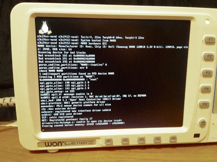
At this point the scope is a fully functioning Linux system with a working display, USB host, USB device, NAND flash and ethernet. Not bad for for a few evenings playing around with it:
If I wanted to it should be possible to write a custom bootloader for the S3C2416 and make Linux boot from flash.
I’m also cheating a bit because I’m skipping the part where I reverse engineered the file system to get the files needed to disassemble the firmware to get ethernet to work. I ought to have been able to get ethernet to work without the disassembly but having it made it easier.
I might write a bit about all that next time. Or maybe something completely different.
Update: continued here