Capturing ADC data into DDR memory on the SDS7102
This is a post in a series about me poking at the insides of my OWON SDS7012 oscilloscope. You might want to start reading at the beginning.
I’m finally on vacation and have had time to do a bit more work on my custom FPGA image for the scope.
First of all, I’ve managed to make the emulated DDR2 memory on the SoC bus read/write. This means that I can use the fast SoC bus for both controlling the FPGA and to read data out of the FPGA. This is good because it means that everything is fast. The bad part is that I’ve had to hardcode some IODELAYs in the FPGA image. The IODELAYs differ between different production lots of FPGAs so the delays that work on my scope most probably won’t work on someone else’s scope. I ought to figure out how to fix this properly, either by calibrating the delays or by using the DQS strobes instead of delays, but well, I don’t think anyone else has dared to try out my firmware on their SDS7102 scope yet, so it probably doesn’t matter that much.
The most visible thing I’ve done though is that I’ve managed to capture samples from the ADC into the DDR2 memory connected to the FPGA. This means that I can capture up to 64 million samples of data at 1 gigasamples/second. Both fast and deep memory and the same time.
As usual it wasn’t smooth sailing to get here. I first tried capturing data to DDR memory using just the 64 word FIFO in the memory controller but a 64 word FIFO wasn’t quite enough, sometimes the FIFO would become full and I’d drop a few samples. Not good.
When this didn’t work I tried adding a FIFO in between the ADC and the DDR2 memory. This worked better but still dropped samples every now and then. I finally realised that this is because the write full flag (wr_full) of the Xilinx memory controller is registered so I need to wait one clock cycle before it reflects a FIFO full condition. But to keep up with the data from the ADC I really need to write to the FIFO on every clock cycle, so this won’t work. It took some time to realise what was happening, but when I did the fix was fairly easy, look at the FIFO count register (wr_count) and stop writing to the FIFO a few words before it fills up.
I’m also having problems with closing timing, some parts of my design is just too slow according to the Xilinx synthesis tools.
But even with the timing violations it seems to work in real life.
Pretty Graphs
I can now make a capture from the ADC into DDR2 memory on the scope and then extract 1 millisecond worth of data (400 000 samples at 400 megasamples per second and channel), transfer it to a Linux PC, use python to post-process the data and then make pretty graphs like this:
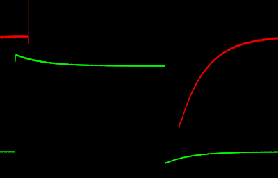
This is with both channels connected to the probe compensation output on the scope. Channel 1 (the red channel) is set for high gain and the signal disappears off the screen at the top. Channel 2 (the green channel) has a lower gain and fits on the screen. I’ve cheated a bit and have offset the channels by 50µs in post-processing to make them easier to tell apart.
As you can see I’ve tried to make the signals look a bit “analog”. On an analog scope a steady signal will stay in place and illuminate the phosphor for a longer time and make the phosphor in that location brighter. A faster changing signal will illuminate the phosphor in each spot for a shorter time and the phosphor won’t be as bright.
Each pixel in this graph represents 1000 samples which are weighted together to decide the intensity of each pixel. If you look at the rising edge of the green signal it is brighter at the top where it’s changing more slowly. The falling green edge and the red edges are changing a lot faster and are also less bright.
The size of the graph is 400x256 pixels. My thought is that if I scale this image to 800x512 pixels it should fit perfectly on the 800x600 screen of the oscilloscope, leaving 88 pixels at the bottom and the top of the screen for the user interface. The weighting algorithm doesn’t try to be accurate and match the behavior of phosphor in any real sense, I’m only trying to make it “look good” and provide some useful information.
I can take the same captured waveform and zoom in a bit and show 1µs (4000 samples) worth of data:

Each pixel represents only 10 samples and the weighting algorithm can’t do as much with the intensity anymore. It’s possible to see that there’s some kind of ringing or noise at the bottom of each falling edge though.
This is a graph at maximum zoom with 100ns (400 samples) worth of data:

There really isn’t any difference in intensity anymore since each pixel represents 1 sample and the weighting algorithm can’t do that much with it. The graph isn’t as pretty anymore, but I’d say it still looks OK. And the ringing from the previous graph is clearly visible.
But…
There’s one big problem with these pretty graphs. They take a lot of post-processing to make. The more data that has to be weighted the slower it is. The first graph with 1000 samples per pixel take about 10 seconds to create on a PC. Of course, this is using floating point in Python which isn’t the fastest language when it comes to processing individual pixels, so it can be optimized. But even then, even rewritten in C i doubt that the ARM CPU in the scope can produce a frame rate of 30Hz if it has to process many thousands of samples per frame.
I do have an idea that it might be possible to do in the FPGA. If I’m lucky that is, it’s quite possible that what I want to do won’t fit in the available logic elements of the scope and then I’ll have to settle for something that isn’t quite as pretty as these graphs.
Yes, another thing. The reason I’m sampling at 400 megasamples/second instead of at 500 megasamples/second (which is the maximum rated sample rate for two channels or a total of 1 gigasamples/second) is that if I increase the sampling rate I start seeing a lot of noise:

It’s not an awful lot of noise, but it’s a lot worse than the clean graphs above at 400 megasamples/second. I’m not sure if this is a digital problem with the ADC outputs (which might be solvable with a few strategical IODELAYs in the FPGA) or if noise, jitter, resonance or something else from some other part of the scope couples onto the actual analog signals before the ADC. For the moment I’ll just run the scope at 400 megasamples/second and be happy with that, but it would be nice to figure out where this noise comes from.
Well, I’ll sit and experiment with visualization algorithms in the FPGA for a while and see what I can do.