The analog frontend of the SDS7102
This is a post in a series about me poking at the insides of my OWON SDS7012 oscilloscope. You might want to start reading at the beginning.
I’ve been home sick from work for a few days and have mostly been sleeping my days away. But now I’m awake in the middle of the night so I thought I’d document what I did last week with the analog frontend of the SDS7102.
There won’t any other pictures in this post so I might as well start with a gratuitous picture of my desk with my disassembled SDS7102 scope.
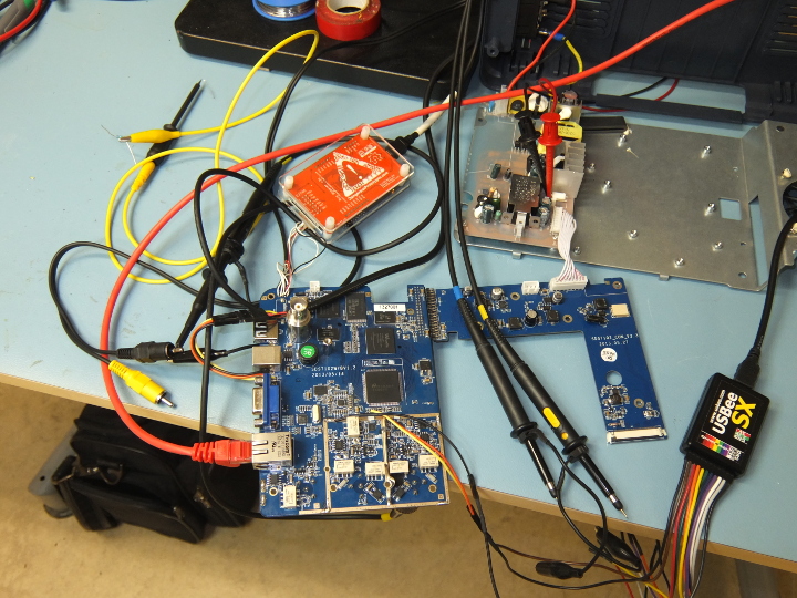
The metal plate to the upper right is the back plate of the scope which holds the power supply. 230V can be lethal and it’s not something I want to risk, instead I’m powering the scope with 7.5V from a bench power supply using two clips on the battery connector. I’ve disconnected the display and the front panel since I don’t need them for most of the things I’m doing.
The two scope probes in the picture are connected to a scope which is not in the picture. The yellow cable to the upper left has a resistor on one end with the other end connected to a sharp multi-meter probe. Hold the resistor against ground or VCC and poke with the probe at an undriven pin to force it high or low.
I’m using a FTDI TTL-232R-3V3 cable connected to UART0 on the scope. A bus blaster MIPS is used for JTAG. The USBee SX is used as a logic analyzer and is hooked up to the SPI bus. The reason that half of the main PCB of the scope hangs outside of the desk is that I have a scope probe plugged into channel 1 on the bottom which then probes an audio signal on the RCA cable. The scope is also connected to the local network using ethernet.
All of these things are connected to a Linux PC which is not pictured. This means that I can log into the Linux PC and do just about everything remotely. I can power the scope on and off using some simple scripts that talk to the power supply over a USB port. I can connect to the serial console. I can use OpenOCD to debug the CPU. I can use just about any audio application to create a test signal to measure. And I can use sigrok to record data from the logic analyzer.
Or I can record data from the logic analyzer once. The sigrok firmware seems to be quite buggy and hangs after doing a capture and the logic analyzer has to be unplugged to restart it. Meh. I guess you can’t get everything. It should be possible to reload the firmware in the logic analyzer and reset it that way but I haven’t figured out how to do that yet.
The analog frontend
What I wanted to do was to figure out how all the control signals from the SoC and the FPGA affected the signals from the frontend. I rebooted the scope with the OWON firmware and did a soft reset and load Linux so the ADC would be running.
I already knew that the solid state relays connected to GPA0 and GPD8 on the SoC controlled the AC/DC coupling on channel 1 and 2 respectively, so I haven’t even bothered checking that.
By just looking at the captured data I quickly realised that the four relays near the channel inputs controlled the attenuation. They have to be switched in pairs and in opposite directions to work. GPA1 and GPA15 are used for channel 1, if GPA1 is high and GPA15 is low it selects low attenuation, if GPA1 is low and GPA15 is high it selects high attenuation which attenuates the signal by 10 times compared to low attenuation. GPH12 and GPE1 do the same thing for channel 2.
Each channel has a four channel MUX which is used to select a signal from somewhere in the AFE which is fed to the trigger circuit for the channel. As far as I can tell three of the four inputs are all fed exactly the same signal and the fourth input is fed something that looks like the output of a differentiator amplifier. I guess this could be useful for triggering on the slope of a signal. Having a four channel mux to select between only two different inputs feels a bit wasteful so I’m probably missing something.
The odd relay at the top of the channel 2 shield box is connected to GPE3 and if high switches the trigger circuits for channel two to the external trigger input. This means that it’s possible to trigger on channel 1 and channel 2 at the same time, or on channel 1 and the external trigger. The relay close to the external trigger input switches between low and high attenuation for the external trigger.
The SPI bus
The ADC, the ADF frequency synthesizer used to create the sampling clock for the ADC, the Rohm DAC and the two LMH variable gain attenuators for each channel are all connected to a SPI bus from the FPGA. I could probably have figured out the configuration for all these devices by reading the data sheets but I was getting a bit lazy so I soldered some wires onto the SCK and SDO wires of the SPI bus. After a lot of curses about sigrok, it had problems keeping up with the data rate from the logic analyzer and would often stop capturing and also had to be unplugged after each capture, I finally managed to capture the all data transmitted over the SPI bus when the OWON firmware booted up.
I then annotated the transfer log with information about what each access did:
24 bits 0x000000c9 LMH
24 bits 0x000fe100 ADF
24 bits 0x0000fa02 ADF
24 bits 0x00020000 ADF? strange value
24 bits 0x00247bc3 ADF? strange value
24 bits 0x000000c7 LMH
32 bits 0x001b89ff ADC reg 0xb -> 0x89ff
32 bits 0x001a007f ADC reg 0xa -> 0x007f
32 bits 0x001dffff ADC reg 0xd -> 0xffff
32 bits 0x001effff ADC reg 0xe -> 0xffff
24 bits 0x000000d7
32 bits 0x001389ff ADC reg 0x3 -> 0x89ff
32 bits 0x0012007f ADC reg 0x2 -> 0x007f
32 bits 0x001dffff ADC reg 0xd -> 0xffff
32 bits 0x001effff ADC reg 0xe -> 0xffff
24 bits 0x00107681 ADF? strange value
24 bits 0x000000c7 LMH
32 bits 0x001b89ff ADC reg 0xb -> 0x89ff
32 bits 0x001a007f ADC reg 0xa -> 0x007f
32 bits 0x001dffff ADC reg 0xd -> 0xffff
32 bits 0x001effff ADC reg 0xe -> 0xffff
24 bits 0x000000d7 LMH
32 bits 0x001389ff ADC reg 0x3 -> 0x89ff
32 bits 0x0012007f ADC reg 0x2 -> 0x007f
32 bits 0x001dffff ADC reg 0xd -> 0xffff
32 bits 0x001effff ADC reg 0xe -> 0xffff
14 bits 0x000012a5 DAC reg 2 -> 0x295
24 bits 0x00247bc3 ADF? strange value
14 bits 0x000012a5 DAC reg 2 -> 0x295
14 bits 0x000012a5 DAC reg 2 -> 0x295
14 bits 0x000012a5 DAC reg 2 -> 0x295
24 bits 0x000000c7 LMH
32 bits 0x001b89ff ADC reg 0xb -> 0x89ff
32 bits 0x001a007f ADC reg 0xa -> 0x007f
32 bits 0x001dffff ADC reg 0xd -> 0xffff
32 bits 0x001effff ADC reg 0xe -> 0xffff
24 bits 0x000000d7 LMH
32 bits 0x001389ff ADC reg 0x3 -> 0x89ff
32 bits 0x0012007f ADC reg 0x2 -> 0x007f
32 bits 0x001dffff ADC reg 0xd -> 0xffff
32 bits 0x001effff ADC reg 0xe -> 0xffff
14 bits 0x000012a5 DAC reg 2 -> 0x295
14 bits 0x000012a5 DAC reg 2 -> 0x295
14 bits 0x000012a5 DAC reg 2 -> 0x295
I had not hooked up the logic analyzer to any of the chip select or load/latch signals of the chips so I had to guess a bit about what each transfer did. From reading the data sheet I knew that the Rohm DAC wanted 14 bits of data for each write so those were easy to identify. The ADC wanted 32 bits and those were also easy.
Unfortunately the two LMH6518 variable gain amplifiers and the ADF4360 frequency synthesizer all wanted 24 bits and they were harder to tell apart. But the high 9 bits of the LMH6518 data should be 0 so all the transfers of 0xc9, 0xc7 and 0xd7 were probably to them and the rest would be to the ADF4360.
I wrote my own SPI master for the FPGA which could be controlled from the SoC. The first thing I did was to talk to the Rohm DAC. It was fairly easy to realize that the bit order of the Rohm DAC was reversed so I had to reverse all the data I transferred to it. Why OWON did things this way I don’t know since the Rohm DAC has a pin which controls the bit order and they could just have set it the other way. I guess they did it that way do begin with and couldn’t be bothered to change it. Anyway, writing 0x100 to channel one of the Rohm DAC produced an output voltage on AO1 of almost exactly 1V, 0x200 produced 2V and so on up to 0x3ff which produced 4V.
Since I could see the frequency from the ADF frequency synthesizer on with my edge counter on the FPGA I tried to configure it next. It didn’t work. I realized that it latched on a different edge so I changed my SPI master to work with it and finally managed to change the clock frequency.
I then went on to the LMH variable gain amplifiers and saw that the amplitude of the signals from the ADC changed when I changed their configuration.
Finally I managed to configure the ADC. The simplest change I did was to switch between sampling one scope channel with both channels of the ADCs and sampling one scope channel with each channel. This was easy to see in the data captured from the ADC.
Then I tried to put all this together and of course nothing worked. Sometimes I could change the configuration for the LMH amplifiers, sometimes not and sometimes the ADF frequency synthesizer just went mad. I spent a lot of time wondering if my SPI master was subtly broken. In the end I realised that the different chips all have different requirements on clock polarity (CPOL) and which edge data should be changed on (CPHA) and how the chip select or load/latch signals should look. Read here for more on the different SPI transfer modes.
I rewrote the SPI master completely so that it had some configuration bits for CPOL, CPHA and the chip select or latch/load signals which could be set per transfer and this finally made everything work. I could finally change the gain of the LMH amplifiers, switch the frequency of the ADF frequency synthesizer and change the ADC configuration. Success.
I also found out that the first write of 0x000000c9 wasn’t to the LMH, it’s to the ADF frequency synthesizer. And that some of the writes I’ve labeled as ADF don’t look correct, the values are just strange.
Then the ADC stopped working. After spending too much time looking at my FPGA code I found out that the wire I had soldered from the logic analyzer to a resistor from the SCK line to the ADC had pulled so hard on the joint that it had broken the surface mount resistor. Oops. Luckily enough it was easy to desolder the resistor and replace it with a new one.
Back to the analog frontend
The outputs from the two trigger MUXes are fed to the two inputs on a dual PECL comparator. After probing around a bit I could see that AO1 and AO2 from the Rohm DAC ended up as the reference voltages for the comparators. So that’s how you set the trigger voltage. Nice.
I was unable to find out what the other channels from the DAC are used for. Most strangely, none of them affect the vertical position of the signal in the captured data from the ADC. Something is not right here.
After a lot of head scratching I realised that the mystery chip U16 had a couple of analog voltages on pin 3 and 4. It must be a DAC of some kind. When I searched for D32E+DAC I immediately found the page for the TI DAC8532 16-Bit, Dual Channel, DAC and the pinout matched. Why on earth didn’t I find it before? I must have been blind.
This also explains the writes of strange values to the ADF4360 in the SPI transaction log above. They were writes to the DAC8532. After forcing the chip select pin of the DAC8532 low and looking for edges on the FPGA I found that it was connected to pin A8 on the FPGA. I added support for the new chip select in my SPI master and, yes! I was able to change the output voltage of the DAC and this also changed the vertical position of the signals from the two scope channels. Probing the U3 OP-AMP below the DAC8532 is used to scale/shift the voltage and increase the drive capability of the DAC. That’s one mystery solved.
As far as I can tell only 2 out of the 10 outputs of the Rohm DAC are used. This seems a bit wasteful, why not use a cheaper 2 channel DAC of only 2 channels are needed. I must be missing something here too.
Where were I? Yes, triggering. When looking at a 3 kHz sine wave on channel 1 I could see that pin D5 on the FPGA was changing at 3kHz. Doing the same thing for channel 2 would make T12 switch. The strange thing is that this signal did not come from the PECL comparator. If I changed the trigger voltage from the Rohm DAC so that the PECL output would stop switching I still saw 3kHz on the FPGA pins. Huh?
I had all forgotten about the Rohm BA7046 video SYNC separators. There were two chips, U34 and U35, one for each channel that I hadn’t figured out what they were doing yet. It turns out that they are also fed from the trigger MUXes for each channel. And when a BA7046 is fed a 3kHz sine wave it will output a 3kHz square wave on the vertical sync (Vd) output and a 17-18kHz square wave on the horizontal sync (Hd) output. And those were the 3kHz seen on D5 and T12 and 17-18kHz seen on R12 and E6.
But what about the PECL comparators? I had located all but four pins on the FPGA and those pins were not differential pairs so they could not be fed the signals from the PECL comparator directly. I could not find any other ICs that could do a PECL to single ended conversion and none of those remaining four pins on the FPGA were toggling anyway. How can this work?
I went to bed a bit frustrated. I was this close to knowing everything there is to know about how the scope is put together and was stumped on this last little tiny thing.
When the light went on it nearly blinded me. I had messed up the location of a FPGA pin before, hadn’t I? What if I had done it more than once? What if the to differential outputs from the PECL comparator were actually connected to two differential inputs of the FPGA? The PECL signal levels are so high that both a low and high PECL level will look like a high signal to the FPGA and they have to be measured differentially to show any toggling.
Of course. I had put down B6 as the pin for the SDA line to the AT88SC CryptoMemory. It was actually part of the B6/A6 pair connected to the channel 1 differential output from the PECL comparator and C9/A9 was connected to the channel 2 output. The AT88SC SDA was actually on C5. With this change I could finally see 3kHz on both pairs of pins on the FPGA and could make them stop switching by changing the trigger voltages from the Rohm DAC. Doh.
Success?
I’m done.
I have discovered almost everything there is to find out about the scope. I know what every single pin on the FPGA does and what most of pins on the SoC do. I know how the analog frontend works, I can control the attenuation, gain, levels, triggers and sampling frequency and can capture samples from the ADC.
Ok, there are few things such as why they are using a 10 channel DAC or 4 channel MUX when they only use 2 channels. There is one pin, GPB6, on the SoC that keeps changing every now and then and I have no idea why it does that.
This means that I’ve probably missed something.
But I know enough about how the scope fits together that I should be able to actually write a new firmware for it from scratch. It may be hard to get the fast DDR bus between the SoC and FPGA to work, and it may be hard to make the DDR memory connected to the FPGA work since it breaks the Xilinx MIG design rules, but it should be possible.
There’s a big risk that I won’t do that though. Most of the the fun with this has been to figure out how everything works. To actually write a polished GUI for a scope and all the small pieces that are needed isn’t quite as fun.
But I’m going on vacation in august and if it rains a lot I might get a bit bored. Who knows. :-)
Update: I’ve put the source code for my Linux port and FPGA image on github.