The SoC bus on the SDS7102
This is a post in a series about me poking at the insides of my OWON SDS7012 oscilloscope. You might want to start reading at the beginning.
In my last post I had managed to capture some data from the ADC and make a bit of sense of it. Since I now had a way of capturing data in the FPGA, why not apply it to the pins connected to the SoC?
As I had discovered earlier the FPGA is connected to the DDR2 memory bus of the SoC. I believe that the FPGA simulates a DDR2 memory. This is bad because the DDR2 bus is rather complicated.
The good thing is that I should be able to write some code on the SoC that affects the signals on the SoC bus which should make it easier to figure out which pins do what. For the ADC bus where I had to make do with whatever the ADC gave me, now I can control the data.
The DDR2 memory chip has the following signals:
- /CS - chip select (active low)
- /RAS - row address strobe (active low)
- /CAS - column address strobe (active low)
- /WE - write enable (active low)
- BA0..BA1 - bank address
- A0..A12 - address
- DQS0..1 - data strobe
- DM0..1 - data mask
- DQ0..15 - data
- CKE - clock enable
- ODT - on die termination
Adding all these together makes a total of 41 signals. I had only identified 38 signals for the SoC bus so something is missing. I guess CKE and ODT are optional, but there’s still one signal too many.
Oh well, lets get started.
Data signals
The first thing to do was to write some test code for the SoC which would run directly after starting a capture of the SoC pins:
for (i = 0; i < 32; i++)
    writel((1<<i), soc_mem + i * 4);
The idea is to move a 1 bit across a 32 bit word and see if I can find that pattern in the capture. “soc_mem” is the address assigned to the second DDR2 memory connected to the SoC.
Here’s a capture of those signals:
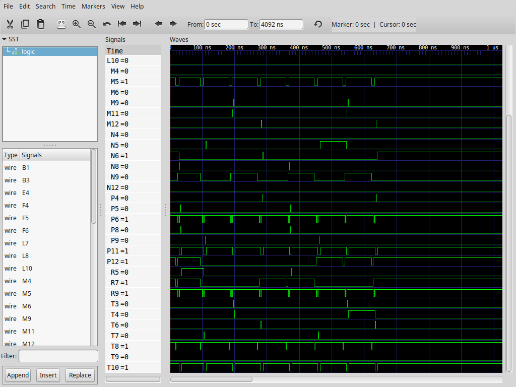
Looks kind of messy doesn’t it?
But if I just move the signals around a bit and give them sensible names it looks a lot better:
Yes, that’s clearly a 1 bit moving through the data signals. Since DDR2 bus is only has 16 data signals the pattern repeats twice. The other signals are control signals or address signals.
It’s interesting that the SoC sometimes turns off the data signals when it’s done with them and sometimes not. Or maybe the SoC has just three-stated the data signals and the voltage hasn’t dropped yet. It shouldn’t matter that much though.
I later realised that the numbering of the DQ signals is wrong, the CPU does write buffering and reordering of writes which means that the writes are not in made the same order as done from my test code. But that doesn’t matter too much, for the moment all I need to know are which pins are the data signals, I can always sort out the exact ordering later.
Address signals
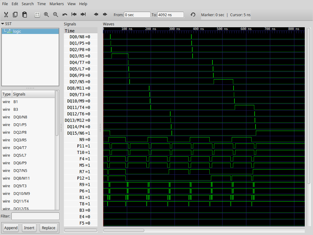
I should be able to do something similar for the address signals if I change the stride for the address. Since the writes are buffered and can change order I decided to use reads instead:
for (i = 0; i < 64; i++)
    readb(ddr_mem + i * 2);
I then tried this for lots of different strides for the address. At first I couldn’t make A0 toggle and finally realized that that’s because the DDR2 memory bus always does burst transfers and the CPU seems to align those transfers to 32 bit words. With a 16 bit memory this means that the lowest address bit will never change.
After a lot of tries and thinking I ended up with this code:
for (i = 0; i < 64; i++)
    readb(ddr_mem + i * (2048 + 64 * 2048));
My capture buffer in the FPGA was just large enough to capture 64 memory accesses so that’s how many loops I have.
The settings for the memory controller in the SoC look like this:
RASBW1 = 2'b10 -> 13 bit
CASBW1 = 2'b10 -> 10 bit
ADDRCFG1 = 2'b01 -> {RA,BA,CA}
This tells us that the row address (RAS) is 13 bits wide, the column address (CA) is 10 bits wide, and that the order those addresses are pasted together to make up the memory address on the SoC. The bank address (BA) is hardcoded to two bits.
With a 16 bit wide memory and 10 bits of column addresses a stride of 2048 should avoid toggling the column addresses. The low bank address signal (BA0) should toggle for every access. The high bank address signal (BA1) should toggle for every other access. With 64 steps the loop will change 6 bits so the next 4 address signals A0, A1, A2 and A3 should also toggle. And if I add one more stride of 64 * 2048 at the same time I should be able to also toggle the next 6 row address lines: A4 to A9.
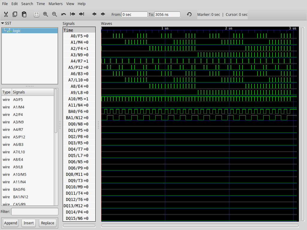
Well, look at that.
BA0 is toggling for every read. BA1 is toggling at half that rate. A0 is used for both the row address and the column address so that wire just shows short spikes when it’s writing the row address before it switches to writing the column address which is always zero. But the length of the bursts of spikes on A0 is twice as long as the pulses on BA1. It continues this way all up to A9 as expected.
A10 is toggling all the time even though my code shouldn’t touch that address signal. But A10 has an alternate function, it tells the DDR2 memory to perform an automatic precharge so that’s probably why it is toggling. A11 is low here since it’s never touched by my code, but I have verified that it will also change if I change the stride to 128 * 64 * 2048.
It also seems that the OWON designers dropped the highest address line A12 from the SoC bus. I guess they can manage with only 32MBytes of address space for the SoC bus.
Control signals
Only eight signals left.
Quoting a Hynix document about DDR2 memory:
The Bank Activate command is issued by holding /CAS and /WE HIGH with /CS and /RAS LOW at the rising edge of the clock. The bank addresses BA0 ~ BA2 are used to select the desired bank. The row address A0 through A15 is used to determine which row to activate in the selected bank.
After a bank has been activated, a read or write cycle can be executed. This is accomplished by setting /RAS HIGH, /CS and /CAS LOW at the clock’s rising edge. /WE must also be defined at this time to determine whether the access cycle is a read operation (/WE HIGH) or a write operation (/WE LOW).
Lets go back to the writes again and zoom in on a single transaction:
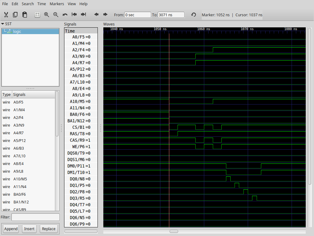
That pretty much looks like it, doesn’t it? /CS and /RAS go low with the BA and A lines low for a Bank Activate command for a row address of 0 in bank 0. After that /CS, /CAS and /WE go low to start a write; A3 and A4 are high saying that the write should be to column address
- The SoC then starts another write, this time A2 is also high indicating a write to address 28. A10 is also high asking for the second write the DDR memory to do an automatic precharge of the bank when the write has finished.
Each write command is for a burst of 4 words and a few cycles after the writes we can see the transfer of the data words with data being transferred twice as fast as the control signals. That’s what the double in DDR, Double Data Rate, means.
The data signals first transfer the low 16 bits of a 32 bit word, where the lowest bit is set, followed by the high 16 bits of a 32 bit word which are zero. The next two transfers are the low 16 bit word with the second lowest bit set followed by the high 16 bit word which is zero. This finishes the first burst of 4 words of 16 bits each. It’s immediately followed by the next second burst of 4 more words.
Note that this is the first write on the bus but the address is 24 not 0 as I would have expected. For some reason the SoC reorderd the writes. This means that my first naive numbering of the DQ lines is wrong, but now that I know the address signals I can use those to fix up the numbering of the DQ signals. I’ll do that sometime later.
I think that DM0 and DM1 are the data masks indicating which bytes of each word should be written, DM0 says that the low byte of a 16 bit word should be written and DM1 says that the high byte should be written. Since my code is writing full 32 bits words, both bytes should be written in the waveform above. Note that I might have swapped the order of the bytes for DM0 and DM1 but that should be easy to fix if that’s the case.
I’ve named the last two signals DQS0 and DQS1. They are supposed to toggle for each bit that’s transmitted and as you can see they are low all the time in my capture. I have seen them change sporadically in other transactions so I think they actually are the DQS signals but I’m not totally sure.
The problem is that on a DDR2 bus DQS are the byte strobes that should be used to sample the low or high 8 bits of the DM and DQ signals. In my capture I’m capturing everything using the DDR reference clock which is not how you’re supposed to do it, and I’m probably seeing corrupted data.
Finale
I think I have identified all signals on the SoC bus now. It’s definitely the DDR2 memory bus and yes, the FPGA is supposed to emulate a second DDR2 memory chip connected to the SoC. Ouch.
The reason for “ouch” is that a DDR2 memory bus is a bit complicated. A FPGA emulation of a DDR2 memory can ignore most things it doesn’t need such as bank precharge or refresh, but the clocking is really messy. A 16 bit wide DDR2 bus works with three different clock domains, there’s the main DDR clock which is used for the control signals, but then you really have to treat the two DQS signals as clock for the corresponding DM and DQ signals.
There are reasons why the Xilinx Spartan 6 has a hardcoded DDR2 memory controller. It’s tricky to get this right and even trickier to make it go fast. Obviously OWON has managed to make this work so it’s not impossible, but I’m not sure if I can manage it.
I guess we’ll see. At least I don’t have to worry about not having anything to learn in my spare time. :-)
Update: A new post is up.