SDS7102 Front Panel
This is a post in a series about me poking at the insides of my OWON SDS7012 oscilloscope. You might want to start reading at the beginning.
I lied. I had material for one more post about the front panel so I might as well write something about it before I forget what I was doing.
In previous posts I had discovered that pins GPF3, GPH3 from the SoC and pins A5, B5, B8, C6, and D6 from the FPGA were connected to the front panel connector.
Keys
The contributor “lemon” on the EEVblog forums had taken some nice photos of the Front panel PCBs. Here’s a zoomed in image of the active circuitry on the front panel.
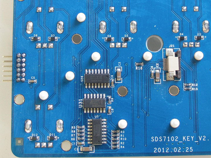
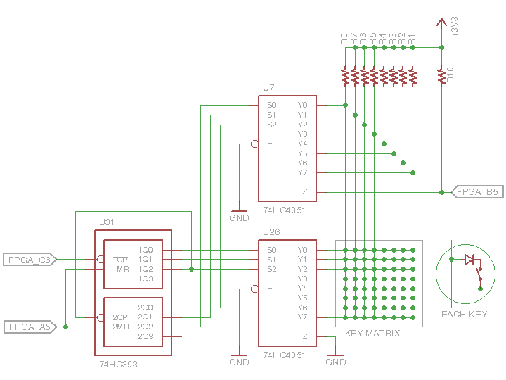
U31 is a 74HC393 Dual 4-bit binary ripple counter. U7 and U26 are 74HC4051 8-channel analog multiplexer/demultiplexers. The traces are clearly visible from the image and even without seeing the traces on the back it is possible to deduce how the front panel works. Here’s how everything is connected:
Simple and sweet.
The keys are arranged in a matrix. (In the schematic that is, the physical layout of the keys is different - some keys are even on a separate PCB). Each key consists of a a switch which can connect a column to a row through a diode. Some of the keys are actually rotary encoders, but at this level they can be seen as simple keys.
The three low bits of the first counter control mux U7 and selects a column (Y0-Y7) that will be connected to FPGA pin B5 through the common pin (Z).
The three low bits of the second counter control mux U26 and selects a row (Y0-Y7) that will be shorted to ground through the common pin (Z).
Normally all columns are pulled high by resistors R1-R8. If a key is pressed and the row it is connected to is shorted to ground, the whole column will be pulled low. If that column is selected, the output to the FPGA will be the same as the state of the column.
FPGA pin C6 outputs a 312.5kHz clock which increments the first counter. When the first counter wraps around it increments the second counter. By toggling FPGA pin C6 and reading FPGA pin B5 it’s possible to read the state of all 8x8 = 64 keys. FPGA pin A5 is used connected to the Master Reset (MR) pins of the counters so that it can restart the counters from zero.
Bits and bobs
The remaining pins of the front panel connector control the lights in the buttons on front panel.
FPGA pin B8 controls the white LED in the Single button.
FPGA pin D6 controls the red LED in the Run/Stop button.
SOC pin GPF3 controls the green LED in the Run/Stop button.
I have no idea why they decided to use a SoC pin for the green LED and why the other two LEDs are controlled by the FPGA. It probably made sense at the time.
This still leaves one pin unaccounted for. SoC pin GPH3 is also routed to the front panel connector. I could not find that pin anywhere on the front panel.
But there’s something that looks like a small window for an infrared receiver on the front of the scope. And there’s space for some more components and through hole mount component with three pins on the PCB just beind the window.
SoC pin GPH3 is the receive pin for serial port 1 and the UARTs do support IrDA. Doh! Of course!
I haven’t actually verified that GPH3 ends up here and I can’t get to the pads on the board without unscrewing the whole panel which I’d prefer not to do, but I bet that’s it. I guess someone at OWON had plans for adding an infared remote control to the scope but that the plans were scrapped and they just decided to just not mount the components for it.
Update: A new post is up.