Finding SDS7102 GPIO pins
This is a post in a series about me poking at the insides of my OWON SDS7012 oscilloscope. You might want to start reading at the beginning.
In my last post I opened up the scope to take another look at the components. That post was a bit long and boring wasn’t it? Just a list of components and guesses at what they might do. But it gave a me a list of things I wanted to find on the main board.
It was time to get my hands dirty and actually find things.
From the register dump I had a extracted a list of GPIO pins that were configured as outputs. One of the first things I did was to toggle these pins just to see what happened. One pin turned out to control the brightness of the LCD display. A few other pins made things click inside the scope. Yet another pin, GPF3, made the Run/Stop button light up in red. What might the other outputs do?
Trying outputs
I did the same thing with changing outputs again, just a bit more systematically.
I started with GPA1, the first GPIO pin that had made something click inside the scope. I set up a small loop that toggled the pin every second:
# Use /sys gpio support to export GPA1 to userspace
echo 1 >/sys/class/gpio/export

# Make GPA1 an output
echo out >/sys/class/gpio/gpio1/direction

# Toggle GPA1 every second
while sleep 1; do
    echo 0 >/sys/class/gpio/gpio1/value
    sleep 1
    echo 1 >/sys/class/gpio/gpio1/value
done
I could hear clicking coming from one of the relays but it was hard to pinpoint exactly which relay was changing just from the sound so I had to probe the pins of each relay with a multimeter instead.
GPA1 turned out to control one of the relays for Channel 1. From my disassembly of the oscilloscope firmware I had seen that GPA12 and GPA15 were often changed at the same time and tried those pins next. I still haven’t figured out what GPA12 does yet, but GPA15 is the other relay for Channel 1.
I then went through the whole list of pins configured as outputs and then probed most of the components in the AFE, sometimes guided by the disassembly which let me make some guesses as to what might be affected by a pin. For example GPA0 and GPD8 are modified near each other and turned out to control the two solid state relays.
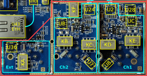
Here’s the list I finally came up with:
GPA0    Channel 1 solid state relay (U8)
GPA1    Channel 1 mechanical relay (KE)
GPA15   Channel 1 mechanical relay (KD)

GPD8    Channel 2 solid state relay (U7)
GPE1    Channel 2 mechanical relay (KC)
GPH12   Channel 2 mechanical relay (KB)

GPC7    External trigger mechanical relay (KA)
GPE3    Mechanical relay with unknown function (KF)
In the disassembly GPC7 and GPE3 are modified near each other, This means that there’s a high chance that the unknown relay controlled by GPE3 also has something to do with the external trigger input.
As an added bonus I also found the buzzer output:
GPB0 Buzzer
I thought I had tried out GPB0 already, but must have made a mistake earlier. It’s important to double check everything. Since GPB0 can also be configured as a timer output it should be easy to make it play beeps at different frequencies.
This was getting a bit tedious though. Finding every pin this way would be extremely time consuming, more than one hunded GPIO pins times tens of interesting component pins makes a couple of thousand combinations to try. Not fun at all. And just changing output pins wouldn’t help me find any input pins either.
Work smarter, not harder
To speed this up I wrote a small Linux device driver which configures all unknown GPIO pins as inputs with a pull up. The driver then sits in a loop reading the GPIO data registers and checks for any change in the value. If the driver sees the bit representing a pin change it prints a message to the Linux console.
I first measuerd the voltage of the A0 pin on the Channel 1 MUX (U31 pin 8), it was at 3.3V, good. I then shorted the A0 pin to ground with a wire. Phew. No sparks and look what appeared on the Linux console:
GPCDAT 0x0000007c -> 0x0000005c diff 0x00000020
GPCDAT 0x0000005c -> 0x0000007c diff 0x00000020
Looking at the values I could see that bit 5 of the GPCDAT register went low when I touched the pin with the wire and went high again when I removed the wire. The SoC has a weak pull up on the pin which makes it high, by touching other end of the trace at the A0 pin I’m forcing the whole trace low. This means that is is very probable that GPC5 is connected to pin A0 on the MUX.
Actually I didn’t just use a wire to ground, shorting an actively driven output to ground can fry the driver, or short the whole power suply if it turns out to be a power rail. Instead I connected my wire to ground via a 330Ohm resistor. For a pin which is at 3.3V, a 330Ohm resistor will limit the current to 10mA. This current is low enough that it probably will not not fry anything immediately. There’s still a risk that I’ll fry something but it should be fairly safe to probe unknown pins this way as long as I don’t force a pin for too long.
Using the driver to check inputs made finding connections a lot faster. I quickly found the connections for all the other MUX pins.
GPC5    Channel 1 MUX A0 (U31 pin 8)
GPC6    Channel 1 MUX A1 (U31 pin 9)
GPH9    Channel 2 MUX A0 (UE pin 8)
GPH11   Channel 2 MUX A1 (UE pin 9)
(Note to self, I think I’ve forgotten to check the shutdown and enable pins. I believe that they are hardwired, but I’d better check.)
More pins
I continued first measuring and then forcing pins to ground all over the place to see what happened. It’s a good idea to measure the voltage on pin before trying to force it. If the pin is already at 0V there’s no use in trying to force it low. If the voltage is higher than 3.3V it shouldn’t be connected to the SoC or the FPGA since they can’t handle higher voltages than that.
If the pin is low it might still be connected to a pin on the SoC. It might just have a stronger external pull-down than the internal pull-up inside the SoC. In that case it’s possible to connect the wire through the resistor to 3.3V or 1.8V and see if it’s possible to force it high instead. It’s also possible to turn on the internal pull-downs in the SoC and try to force pins high.
I found that GPF3 was connected to resistor R174 close to the front panel connector. Which wasn’t too strange when I stopped to think about it, toggling GPF3 made the Run/Stop button light up so it had to be wired to the front panel somehow. GPH3 was connected to resistor R80 next to it, but nothing happened on the front panel if I changed it. None of the other pins the connector seemed to do anything.
The mystery connector U60 turned out to be a lot of GPIO pins from the SoC. I guess this is just some kind of debug connector where they put a lot of unused pins:
 1      GPL8
 2      GPE8
 3      GPE10
 4      GPH2
 5      GPF7
 6      GPB5
 7      GPH5
 8      GPF4
 9      GPG3
10      GPG1
11      GPG5
12      GPK9
13      GPK14
14      GPK10
15      GPK12
16      GPK3
17      GND
18      GND
19      7.3V, not the same wire as for pin 20
20      7.3V, not the same wire as for pin 19
Note, the GPK pins are all at 1.8V, the rest are at 3.3V. I have no idea where the 7.3V comes from and if there’s any difference between pin 19 and 20 or not. Update: Of course. I’m powering the scope with 7.5V from a power supply into the the battery connector. 7.3V is probably that voltage measured with an uncalibrated multimeter.
I’m a bit sad that the OWON engineers didn’t arrange the GPIO pins from the Soc a bit differently. It should have been have possible to rearrange pins so that all the pins for a SD/MMC interface would be available in the connector. Or or least have a complete serial port or maybe an I2S interface (I2S is a sound bus). It’s of course still possible to bitbang a lot of protocols using the pins but it’s going to be much slower than if they had brought out the proper hardware assisted interfaces.
GPF2 which is used as a VBUS detect for the USB device port was a bit tricky though. I had found it earlier when I just tried ports randomly. When I tried connecting and disconnecting a USB cable with the my driver running nothing happened. Had I made a mistake earlier, didn’t I see this pin change? I finally realized that VBUS is fed into a voltage divider where the divided voltage is then fed to GPF2. With the internal pull-up enabled (which my driver does) GPF2 will be pulled high if nothing is connected to the VBUS pin. When a USB cable is connected the VBUS pin will also pull GPF2 high but since it’s already high the driver will not notice anything different. I turned off the pull-up on GPF2 and the VBUS detect started working again. There are many ways to fool oneself and I think I crossed out and rewrote VBUS=GPF2 at least three times before figuring this one out.
Another strange thing is that the driver reports that GPB6 is changing every now and then. I haven’t been able to correlate this with anything I’ve done so what this pin does remains a mystery.
Summary
Forcing the GPIO pins and looking at what inputs change wasn’t too hard and gave me the locations of lots of pins. Of course I made a lot of mistakes on the way. To begin with I had missed the register configuration for GPH2 so when I first shorted that that pin nothing happened and I thought pin 4 was unconnected. I also lost track of where I was a couple of times so I had to start over. Sometimes I just messed up and managed to short a power supply pin to ground and there would be sparks and the scope would die. Not really recommended.
Also note that some GPIO pins such as the ones in the GPA bank can only be configured as outputs, not as inputs. For those pins I had to try to discover their functions the slow way, by toggling the output and probing every pin that it might be connected to on the PCB.
The variable gain amplifiers, DAC (U2, U24), ADF4360-7 clock generator (U97), ADC08D500 ADC (U37) and AT88SC CryptoMemory (U38) did not seem to be connected to the SoC.
I’ve been unable to locate a couple of the GPIO pins referenced in the firmware such as GPA12, GPA5, GPA7, GPG2 and GPH13. I hope they don’t do anything important.
Still a lot of progress though. And a much shorter blog post where more things happened than the last one. A lot better, innit?
Update: This series is continued here.