Finding SDS7102 FPGA pins
This is a post in a series about me poking at the insides of my OWON SDS7012 oscilloscope. You might want to start reading at the beginning.
In my last post I used a trick where I configured all unknown GPIO pins as inputs and wrote a device driver to detect if the pins changed. This worked so well that I decided to do the same thing using the FPGA in the scope.
The FPGA in the SDS7102 scope is a Xilinx Spartan 6 XC6SLX9.
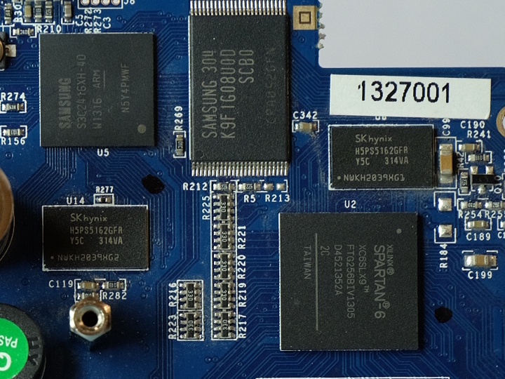
It has an integrated memory controller on bank 3 which physically located at the top of the FPGA in the image above. This memory controller is hopefuly connected to the Hynix DDR2 memory just above the FPGA. Bank 2 is on the left side of the FPGA and is probably connected to the SoC via the resistors to the left of the FPGA. Bank 1 is on the bottom and it’s possible to see a lot of differential traces heading downwards towards the ADC (which is nos in the picture). Bank 0 is on the right and there is nothing obvious that it is connected to. But that’s the whole point of reverse engineering, to find things out, isn’t it?
FPGA programming
A FPGA is a piece of programmable logic. Depending on how you look at it, a FPGA is either totally different from programming, it’s reconfigurable hardware, or a FPGA just another programming language, albeit very different from most normal programming languages.
It is possible to configure an FPGA at the gate level, defining combinatoric logic with AND, OR, XOR gates, inverters, latches and flip-flops. It’s much more common to use a hardware description (HDL) language such as Verilog or VHDL. These languages are often called register-transfer level (RTL) since they use an abstraction of transfers of signals between registers and logical operations on the signals.
I did play around a bit with Verilog a few years ago but have never really come to terms with the language. As a “softie”, someone who comes from the software side, Verilog feels very primitive. The Verilog syntax is a bit inspired by C but it’s even more low level than C if you can believe that. For example, Verilog doesn’t even have anything like a struct. Try to imagine programming C without the ability to collect related variables in a struct, and having to pass each member as a separate argument to a function. It’s not uncommon to have Verilog modules with tens or even hundreds of signals as arguments.
You can combine multiple signals into one big bit vector, but it’s a bit like having to pack a structure into an integer array by hand so that it can be passed through a C function interface, and then having to unpack it by hand again. Rather painful I’d say.
Systemverilog, an extension of plain Verilog, is supposed to solve all of this, but many vendor tools such as Xilinx ISE (the free tool from Xilinx that works with the Spartan 6 series of FPGAs) do not support Systemverilog. VHDL is more complete, it does have “entity” which are interfaces somewhat similar to C structs. The only problem is that I do not get along with VHDL at all. The syntax seems to be inspired by ADA and, well, I just don’t like it.
Because Verilog is so a primitive, people have built lots of tools to automatically generate Verilog from other languages. A few years ago I found something called MyHDL which uses the Python language to generate Verilog or VHDL which looked very interesting and I’ve been meaning to try it out ever since.
I like Python, I even ported Python 1.2 to VMS over 20 years ago. Damn, that’s scary, am I really getting that old? Anyway, where was I? I like Python and being able to program an FPGA in Python sounds really nice. This seems like a a perfect opportunity to learn MyHDL.
I also found something called Rhea. It is a set of useful libraries for MyHDL and it also contains some very nice build scripts for many different FPGAs.
Lots of new toys to play around with and learn.
Hello World
The FPGA is configured by the SoC using five GPIO pins. Three of those pins on the FPGA can be used as general I/O after the configuration is done. The first thing I wrote was the FPGA version of Hello World, a small piece of MyHDL that just toggles one of those I/O pins every second. I used the STARTUP_SPARTAN6 primitive to activate the internal 50MHz configuration clock in the Spartan 6 which then clocks a counter which toggles the I/O pin every time it wraps around. I built an FPGA image using the Rhea build system and then used my FPGA device driver to configure the FPGA and load the image.
After loading the image I could use the Linux device driver I wrote last time and see that the pin changed. The FPGA was alive at least.
Reading FPGA I/O pins
The next step was to configure all the I/O pins on the FPGA as inputs with a pull up and then write some MyHDL code which used the three free pins from the configuration interface to do something more advanced. One pin was turned into a LOAD signal, when that pin changed from low to high (on the positive edge) it would load the state of all 180 or so input pins into a register. Using a second pin as a CLOCK driven from the SoC and the third pin as a DATA OUTPUT from the FPGA, I could then shift out the data from the FPGA registers to the SoC, one bit at a time. I ran a simulation using MyHDL and looked at the signals using GtkWave to see that my code actually did what is was supposed to.
This way I could in theory do the same kind of tests as I had done with the device driver on the SoC, and see the state of each pin configured as an input on the FPGA. This didn’t work as well as for the SoC though, a lot of pins were changing all the time and I didn’t quite know where too start looking. It also turned out that the pull ups on the FPGA pins made the system unstable, Linux would often crash shortly after configuring the FPGA with my FPGA image. Removing the pull ups made the system stable again. Strange, I need to think about that.
Counting edges
My next attempt was to add a counter for each pin that would count the number of times the state of the pin had changed from low to high. With a 32 bit register that would be read every second I should be able to count up to 4 billion changes per second. More than enough since a Spartan 6 FPGA is hard to clock much faster than about 400MHz. And since my counters use the internal 50MHz clock to sample the signal it wouldn’t be able to count faster than that anyway. I couldn’t fit counters for all 180 pins into the FPGA so I had to limit the image to only sample pins on one bank at a time. It sort of worked, some pins would have a count of 0 meaning that they were not changing, one pin changed about 50 times per second but a lot of pins seemed to change as fast as the counter could count and would jump wildly between different values. I wasn’t quite sure if my HDL code was working or if the results were just a lot of glitches. The signals had looked OK in simulation, but I wasn’t sure if my test cases actually covered all the things that would happen in reality.
I did come up with one trick to verify that the counters would work at low speed. I started counting the number of pulses on the clock signal that was used to shift out data. With 55 counters to read, each 32 bits, I should see 55 * 32 = 1760 edges on the clock line for every time I shift out the contents of the counters. But there were usually a few extra edges, the counter would show 1765 or so. Hmm, that’s not quite right.
As a programmer it’s easy to think of digital signals as being digital, a signal is always high or low. That is not true. In reality all signals are analog signals. When a signal changes from 0V to 3.3V this takes time; if the signal is sampled just when it is changing it might be at any intermediate voltage in between. This is a well known problem which is called metastability.
The fix is fairly easy though. Add another flip flop which samples the output from the first flip flop. This gives the output from the first flip-flop time to settle and reduces the risk of metastability. It won’t eliminate the problem completely, but it will reduce the risk to such levels that in practice it will never happen. With this fix I did see exactly 1760 edges for the counter of the clock signal, but a lot of other counters were still jumping around wildly.
Asynchronous counters
What if the inputs to the pins are changing faster than the 50MHz clock I’m using to sample them? That could really give some strange results, couldn’t it? I rewrote my counters one more time so that instead of sampling the signals on the pins the counters would be clocked by the signals on the pins. The Xilinx tools complained about this, it’s bad practice to use signals from pins that aren’t dedicated clock pins as clocks. I had to read up on how to tell the Xilinx tools “shut up, I know what I’m doing” to let me do that. I don’t really know what I’m doing, but well, it did let me synthesize an image that I could load into the FPGA.
Making the counters asynchronous to the internal clock of the FPGA has its own problems. Trying to read a binary counter using a different clock than the counter is clocked risks both metastability or just the risk that the bits in the counter won’t update at exactly the same time. A binary counter which is incrementing from 01 to 10 might have finished changing the low bit from 1 to 0 while the high bit is still changing from 0 to 1. To the reader it would appear as if the counter is 00 and has just counted backwards. Which of course happened. This is also a well known issue, clock domain crossing is a generic term describing the issues when working with signals coming from two different clock sources (domains).
There are also known techniques for transferring signals between clock domains. One such technique is a Gray code where a change of +1 or -1 will only see one bit of the value change and thus avoids the issue with binary counters where multiple bits can change at one time. I added a gray encoder to my counters which converted the value into gray code which was then loaded into the shift register and transferred to the SoC where the gray code was decoded. No more counters that count backwards.
Optimization
I spent the evenings for about one week learning more about MyHDL and optimizing and refining my counters. I wanted to be able to count edges on all pins at the same time but to do that I had to reduce amount of logic needed to do the counting. I found out that I could fit 180 counters into the FPGA if I removed the extra registers used for gray encoding and reduced the counter size to 10 bits. But 10 bits can only count up to 1023 and if the frequency on a pin is 1MHz that means that the counter will wrap around in one millisecond, much faster than I could read the counters from the SoC.
What I finally ended up with was a hybrid counter design where I have 180 counters that are 10 bits wide. Each counter is clocked by the signal from its pin and counts directly in gray code. A counter which counts directly in gray code is not possible to clock as fast as a counter counting in binary, but it uses less FPGA resources (actually, I have to check this, it might not be true).
Since the 10 bit counters can wrap around rather quickly I added a periodic task in the FPGA which loops over each 10 bit gray counter and updates a 32 bit counter in block RAM if the 10 bit counter has wrapped around. With 180 counters counting to 1023 being sampled by a 50MHz clock it should be possible to measure signals with a maximum frequency of 1024 * 50 / 180 = 284MHz on each pin, as long as the gray counters can keep up of course.
Results
The results of all this work is this, a chart with the number of positive edges seen on each pin and the current state of the pin:
  0  C4       0 ^  A4       0 ^  B5       0 ^  A5       0 ^  D5       0 ^
  5  C5       0 ^  B6       0 ^  A6       0 ^  F7       0 ^  E6   17.3k ^
 10  C7       0 ^  A7       0 ^  D6       0 ^  C6       0 ^  B8       0 ^
 15  A8       0 ^  C9       0 ^  A9       0 ^  B10      0 v  A10      0 ^
 20  E7  126.7M v  E8  126.7M v  E10      0 ^  C10  10.0M v  D8       0 v
 25  C8       0 ^  C11      0 ^  A11      0 v  F9       0 v  D9       0 v
 30  B12      0 v  A12      0 ^  C13      0 v  A13      0 ^  F10      0 v
 35  E11      0 ^  B14      0 ^  A14      0 v  D11      0 v  D12      0 ^
 40  E13      0 v  E12      0 ^  B15      0 v  B16      0 ^  F12      0 ^
 45  G11      0 v  D14      0 ^  D16      0 v  F13      0 ^  F14      0 v
 50  C15      0 v  C16      0 ^  E15      0 v  E16      0 ^  F15      0 v
 55  F16      0 ^  G14      0 v  G16      0 ^  H15      0 ^  H16      0 v
 60  G12      0 ^  H11      0 v  H13      0 v  H14      0 ^  J11      0 v
 65  J12      0 ^  J13      0 v  K14      0 ^  K12      0 v  K11      0 ^
 70  J14      0 v  J16      0 ^  K15      0 v  K16      0 ^  N14      0 ^
 75  N16      0 v  M15      0 v  M16      0 ^  L14      0 ^  L16      0 v
 80  P15      0 v  P16      0 ^  R15      0 v  R16      0 ^  R14      0 v
 85  T15      0 ^  T14      0 ^  T13      0 v  R12  17.3k ^  T12      0 ^
 90  L12      0 v  L13      0 ^  M13      0 v  M14      0 ^  T11      0 ^
 95  M12   1.8M v  M11 722.9k v  T10 210.2k ^  N12 104.0k v  P12 977.8k ^
100  N11      0 ^  P11 210.2k ^  N9    3.4M ^  P9  719.6k v  L10 976.7k ^
105  M10      0 ^  R9   13.8M ^  T9   27.3M v  M9  545.1k v  N8  694.1k v
110  P8  807.9k ^  T8  494.4k ^  P7  133.3M ^  M7  133.3M ^  R7  180.8k ^
115  T7  713.9k v  P6  458.5k ^  T6  828.5k v  R5    2.0M v  T5       0 ^
120  N5    1.1M ^  P5    1.9M v  L8  959.5k ^  L7    1.1M v  P4  647.2k v
125  T4    1.2M v  M6   27.3M v  N6    1.6M v  T3    1.1M v  M4  996.0k v
130  M3       0 ^  M5    2.0M v  N4    1.8M v  R2       0 v  R1       0 v
135  P2       0 v  P1       0 v  N3       0 v  N1       0 v  M2       0 v
140  M1       0 v  L3       0 v  L1       0 v  K2       0 v  K1       0 v
145  J3       0 v  J1       0 v  H2       0 v  H1       0 v  G3       0 v
150  G1       0 v  F2       0 v  F1       0 v  K3       0 v  J4       0 v
155  J6       0 v  H5       0 v  H4       0 v  H3       0 v  L4       0 v
160  L5       0 v  E2       0 v  E1       0 v  K5       0 v  K6       0 v
165  C3       0 v  C2       0 v  D3       0 v  D1       0 v  C1       0 v
170  B1  128.4k ^  G6       0 v  G5       0 v  B2       0 v  A2       0 v
175  F4    6.8M ^  F3       0 v  E4  971.0k ^  E3       0 v  F6  115.4k v
180  F5    1.0M v  B3  972.3k ^  A3       0 ^
Whoa. There’s a lot of things happening all the time, even with the FPGA doing nothing. There are a few interesting things in there.
Pin C10 at the line starting with 20 is toggling 10 million times per second. With a bit of luck that is the 10MHz reference clock from the crystal oscillator (U98).
Pins E7 and E8 are both toggling at 126MHz. According to the FPGA data sheet, those pins make up a differential pair and are also a global clock input to the FPGA. This ought to be a differential clock signal from some other part of the scope.
Pins M7 and R7 make up another differential clock input on the FPGA and is toggling at 133MHz. Hmm, these signals are in bank 2 together with a lot of other signals that are changing all the time.
Update: I have managed to swap a few pins in the above chart. At least F7 and E6 should change places. Most of the other pins should be correct.
Nasty surprises
Where have I seen 133MHz before? In the output from the Linux kernel when it is reporting the clock frequencies it is using:
CPU: MPLL on 800.000 MHz, cpu 400.000 MHz, mem 133.333 MHz
What!? You must be *beep* kidding me. What the *beep* were the OWON engineers smoking when they thought that this would be a good idea?
They are using the DDR memory bus as the high speed bus between the SoC and the FPGA. They must have programmed the FPGA to simulate a DDR2 memory. Seriously folks. There is a perfectly usable bus on the SoC which is connected to the NAND flash which is designed to be used as an expansion bus. The expansion bus even supports DMA so that a device on the bus can transfer data directly into RAM on the SoC without even involving the CPU. Why on earth would someone do something as silly as use the DDR memory bus as an expansion bus? But apparently they have, and all those pins changing in bank 2 and bank 3 are the pins from the DDR memory bus. That also explains why enabling the pull ups on the FPGA would crash Linux running on the SoC, doing that messes with the DDR signal integrity and corrupts data in memory.
Ungh. This is going to be a lot harder than I expected.
I’m pretty new to HDL and programming FPGAs. I think my HDL skills should be up to writing an interface that works with the expansion bus of the Samsung SoC; it’s a fairly slow and simple bus. To work with the DDR bus memory, with tight timing and signals coming in on both edges of the clock (that’s what DDR means, dual data rate, data is transferred on both clock cycles) is a lot harder. I feel a bit out of my depth. This is a bit of a showstopper for me.
I think I’ll push on with the reverse engineering anyway. I’m doing this for fun and the challenge and it’s kind of interesting to see how everything fits together. It should still be possible to get everything else to work and be able to sample a waveform and very slowly transfer it to the SoC using the three pins from the configuration interface. It won’t be usable as a proper scope, but it’ll still be interesting as a proof of concept.
Or maybe someone else who is more experienced than me at FPGA programming might be able to do something with the DDR memory interface. Nudge, nudge.
We’ll see what happens.
Update: This series is continued here.