An almost-GHz active differential oscilloscope probe (Part 3)
This is part three of a series about building a active differential oscilloscope probe. Part 1 covered why I wanted a differential probe and the design of it. Part 2 covered actually building the the probe. The probe had much lower bandwidth than I had hoped for but it was still useful.
But well, this was just a first attempt, it should be possible to do better. Here’s the schematics for the circuit again.
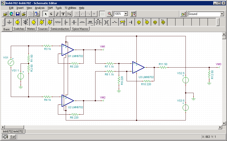
According to simulations it should be possible to replace R3 and R4 with 0Ω resistors and get much better bandwidth. So I tried.
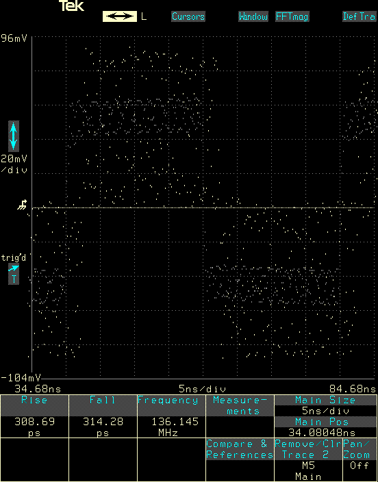
It did not work well at all. It’s possible to recognize the square wave from the input signal but there’s loads of ringing. If you look at the gray signal which is the source you can see that even the source signal is affected by the ringing. Scratch that idea.
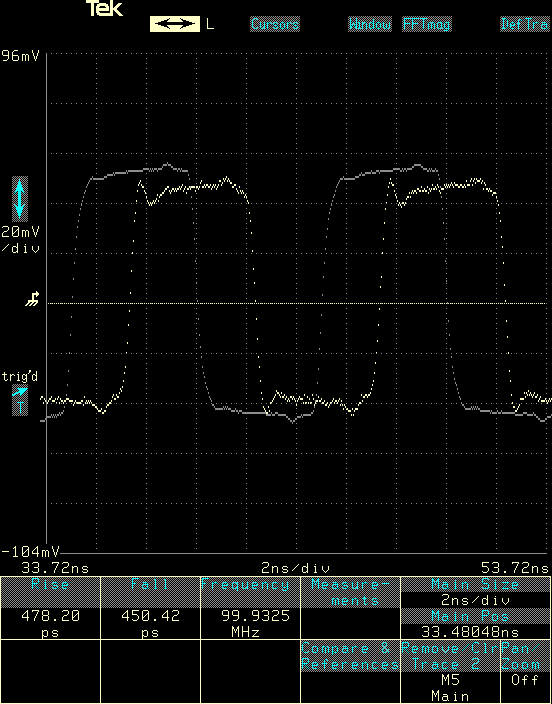
Next I tried a 100Ω resistor. The lighter white trace is the signal out of the probe and it looks decent at 100MHz. There’s a bit of ringing, but not too bad.
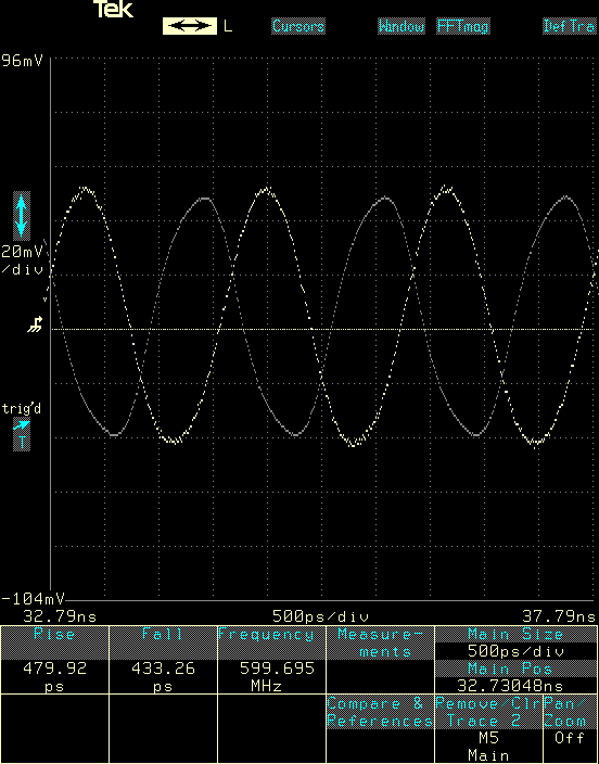
At 600MHz the signal out of the probe is actually stronger than the source signal, This means that the gain at 600 MHz is higher than at 100 MHz. This worried me a bit, the probe might become unstable if the gain at high frequencies becomes too high.
After some more testing, trying 120Ω and 220Ω at the input and also variying some other parameters I finally settled on 150Ω for R3 and R4 as a decent compromise between being happy with the bandwidth and not seeing too much ringing. All other components have the original values from the simulation.
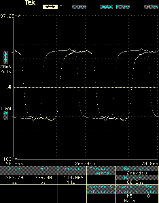
At 100MHz the probe looks really good, it’s even possible to se the little bump on top which I believe is due to impedance mismatch in the SMA connectors on the cables I’m using for testing.
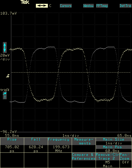
At 200MHz the probe is still doing well.
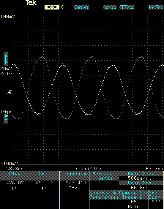
At 700MHz there is a good bit of attenuation but it’s still very good.
At this stage I pestered a colleague into running the probe through a network analyzer to see how it would do. It turns out that the frequency response is almost flat up to 300MHz, the -3dB point is at 850MHz and the -6dB point is at 1.275 GHz.
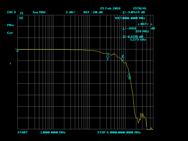
In other words, the probe has a -3dB bandwidth which is more than 800MHz and is actually usable quite a bit beyond 1 GHz.
Mission completed. I’m happy.
If anyone is interested in my Eagle schematics or board files or just has any questions, don’t hesitate to mail me. Contact info can be found below.
Update: I have published the eagle files for the probe on GitHub.