An almost-GHz active differential oscilloscope probe (Part 2)
In my last post I described how I had simulated and designed an active scope probe and sent off the design to a PCB manufacturing house. If you haven’t read part 1 yet you might want to do that before continuing.
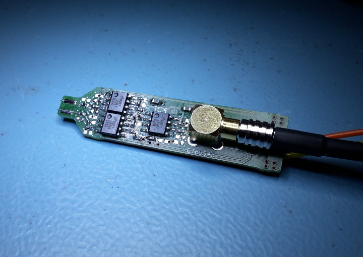
A week later the PCBs arrived in the mail. That evening I assembled the boards. It didn’t take long, there were only about a dozen components to mount.
I first needed something to probe. Luckily enough I had a Si5338 Evaluation Board lying around. This board is powered and controlled from a USB port and can output just about any clock frequency up to 350MHz and selected frequencies up to 700MHz.
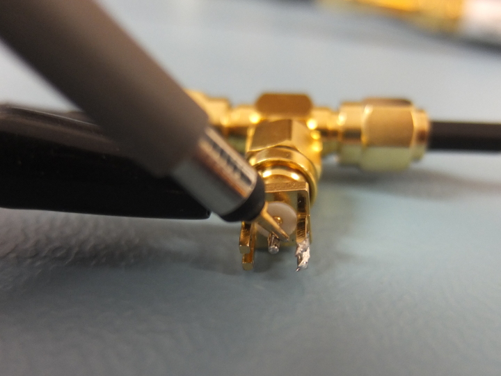
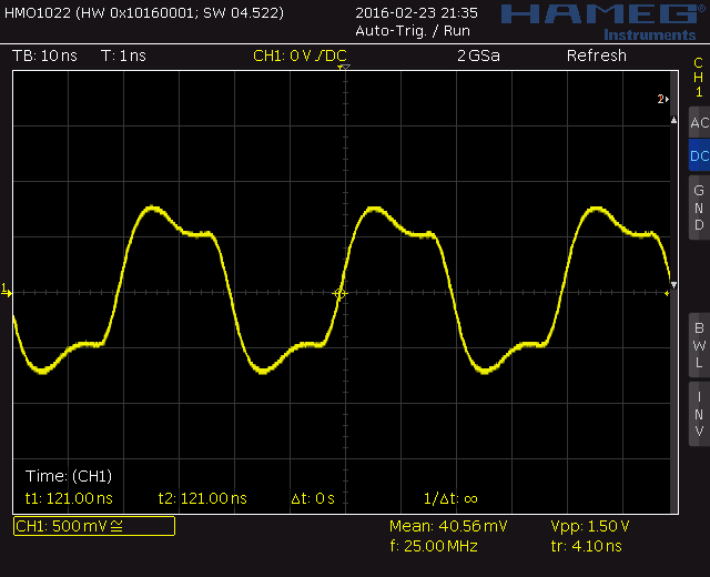
I connected one of the outputs from the clock board to through a SMA “tee” connector directly to an input on my scope. This way I could see the clock signal from the source with as little distortion as possible. As you can see in this screenshot the clock is running at 25MHz and has an amplitude of about 1V peak-to-peak.

Unnecessary details: My old Tektronix 11801B oscilloscope is a bit clunky to use. With the sampling heads I have I can’t trigger directly off the signal I’m looking at. Instead I have to feed the scope a separate trigger signal. I did this by connecting a spare output from the clock board to the trigger input and making sure that the signal I was watching always was a multiple of the trigger signal.
Anyway, I could then use a normal passive scope probe to probe the signal at the “tee” connector.
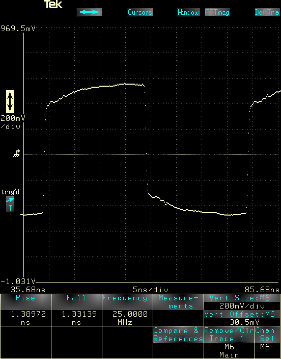
The 11801B can’t use passive probes anyway, the inputs are 50 Ohm only and won’t work with passive probes. Instead I give you a screenshot of my 100MHz Hameg scope with the passive probe above. There’s a lot of overshoot, it’s still possible to see that it is a 25MHz signal, but quite frankly it looks like crap.
A 1:10 passive probe with 10MΩ resistance is perfect for probing slow and weak signals, but the capacitance of such a probe is quite large, this probe is specified to have 18pF input capacitance, and at high frequencies this capacitance distorts the signal being probed a lot. The ground wire of the probe is also fairly long which makes things even worse.
The high capacitance of the passive probe also messes up the source signal. This is how the signal fed directly to the 11801B scope looks when being probed. The loading from the passive probe has really slowed down the signal and changed the shape considerably. And if it’s this bad at 25MHz, imagine what will happen at 500MHz. This could actually make some circuits stop working when they are probed.
It was finally time to test my active probe. The LMH6702 has an input resistance of about 1.4MΩ and an input capacitance of about 1.5pF and unless the parasitic capacitances on the PCB ended up being very large that should be the performance for the whole probe. It means that the probe would have a resistive load which is 7 times bigger than a passive probe, but at high frequencies the capacitance dominates the load and it ought to be at least 10 times lower.
In this screenshot the bright white trace is the signal that comes out of the probe and the darker gray trace is the direct signal from the source.
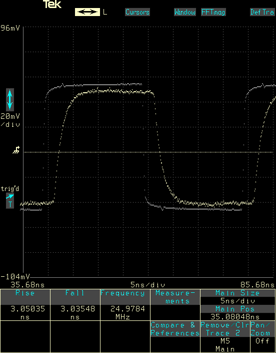
The source signal has barely changed compared to not being probed. At 25MHz the active probe doesn’t seem to load the signal being probed at all. The output from the probe was slower, the almost vertical edges from the source have become a soft slope. But it’s still a lot better than what I got with the passive probe.
The gain for the probe was supposed to be 1:10, so the output from the probe should have had an amplitude of 1V / 10 = 100mV, but I didn’t have any 1.1kΩ resistors for the gain of the second stage and ended up using 1.2kΩ resistors instead. The attenuation ended up being 220/1200/2 or 1:11 and the amplitude about 90mV.
At 100MHz the bandwidth limits of the active probe starts showing a bit. It’s possible to see the rough shape of the source signal in the output from the probe but most of the details have been lost. Also note that there is a constant delay of about 2.3ns, the time it takes for the signal to pass through the OP-amps.
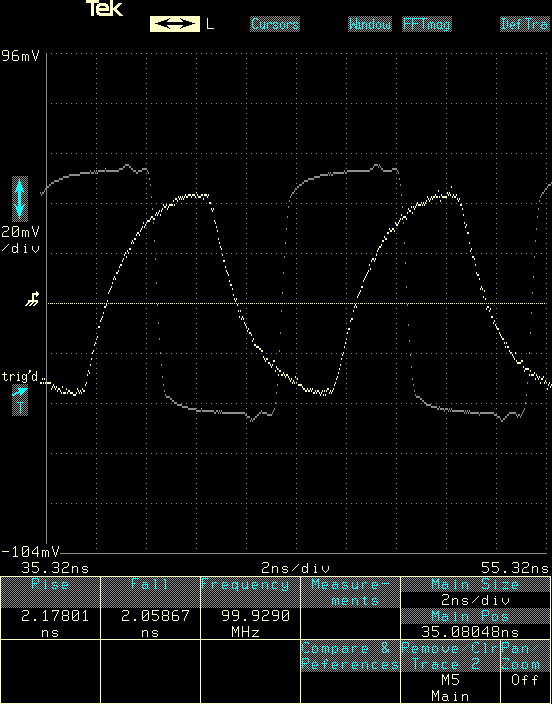
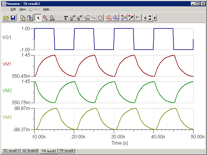
This was actually pretty close to what was predicted by the simulation. Note that in the simulation the input signal is +/-1V = 2V peak-to-peak and the source signal above is 1V peak-to-peak so all amplitudes in the simulation are twice as large.
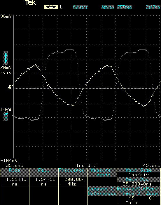
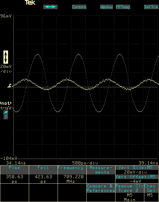
At 200MHz all that was left was a triangle wave and the amplitude out from the probe was markedly lower. This is to be expected as the gain of the probe decreases at higher frequencies.
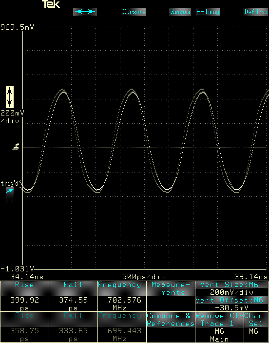
At 400MHz the amplitude was less than half of the source signal. By the way, don’t trust the Rise/Fall measurements the the bottom of the screen, they are quite noisy and jumped around a lot.
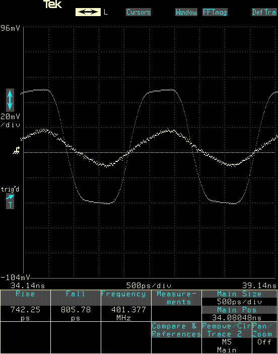
Unfortunately the Si5338 clock generator was unable to output a 500MHz signal so I couldn’t make any direct comparison to the simulation at 500MHz. Instead I cranked the clock generator up to 700MHz, which is almost as high as it can go. The amplitude has halved again.
To get an idea of how much the active probe loaded the source signal at 700MHz I made two measurements and overlaid them on each other. The gray trace is the signal without the probe and the white trace is with the probe. The probe does load the source signal a little bit, it’s possible to tell that the rise time and peak amplitude is slightly slower. It’s actually pretty good though, it’s within 10% and would probably not make any difference and allow most circuits to keep working even when probed.
The bandwidth of a device is usually defined as the frequency at which the gain has dropped by 3dB compared to baseline. Decibel (dB) is a logarithmic unit and -3dB corresponds almost exactly to half the amplitude. For my active prove this happened somewhere between 200MHz and 400MHz and probably closer to 200MHz than to 400MHz.
Update: The previous paragraph is wrong. -3dB corresponds to a halving of power, but since the power is proportional to the square of the voltage, -3dB when talking about voltage is the square root of 0.5 or about 70.7%. This occurs somewhere between 100MHz and 200MHz.
This is far from the 1 GHz bandwidth I would have liked but the probe is definitely very useful anyway. At 500MHz the absolute amplitude is off, but that doesn’t matter that much, I’m usually more interested in seeing the frequency and if there is any jitter on the signal.
At this point I was rather happy. I’m a programmer, not hardware engineer and don’t quite know what I am doing when designing analog hardware. I was slightly surprised that the probe worked at all and was very surprised that it was so stable and useful all the way up to 700MHz.
Good enough for an evening playing around with a soldering iron and then doing measurements with a scope. It was time to call it a night.
Update: This article series is continued in part 3