Capturing data from the SDS7102 ADC
This is a post in a series about me poking at the insides of my OWON SDS7012 oscilloscope. You might want to start reading at the beginning.
I have spent a few weeks learning MyHDL and building FPGA modules that use the Wishbone bus to talk to each other.
The first thing I built was a SPI slave which uses the three wires from the FPGA configuration interface that can be used after configuration. A normal SPI interface uses four wires, an active low Chip Select (/CS), Serial ClocK (SCK), Serial Data Out (SDO) and Serial Data In (SDI). SDO is often called Master Out Slave In (MOSI) and SDI is often called Master In Slave Out (MISO). Anyway, with only three wires I had to combine SDO and SDI into one bidirectional wire SDIO. I tried to modify Linux spi-gpio driver to use a bidirectional SDIO pin but couldn’t see a simple way to do it so I hacked together a dumb Linux driver to do it instead.
The SPI slave is a Wishbone bus master and can control a Wishbone slave connected to it. I converted my MyHDL code that counted edges on pins to a Wishbone slave and made that work with the master. That was fairly easy. The hard part was to write a bus multiplexer which allowed me to connect multiple Wishbone slaves to one Wishbone master. MyHDL doesn’t always work as I expect it to and has a lot of limitations so it took me a few weeks to make all of that work.
With that done it was fairly easy to create a dual port block RAM in the FPGA where one port is connected to a Wishbone slave so that the SoC can read out the data from the block RAM. The other port is connected to the ADC. Using the the ADC clock it captures and stores the 32 differential ADC signals until the RAM becomes full. Another Wishbone slave with a single one bit register is used to stop and restart the capture.
First capture
I used sox on a Linux PC to play a 3kHz sine wave which I then probed with channel one on the scope:
play -n synth 0 sin 3000
I booted the scope with the OWON firmware and made sure that it showed a sine wave on the screen. I then did a soft reset of the CPU in the SoC and loaded Linux. Doing a soft reset leaves the ADC running and this is how I discovered which pins were connected to the ADC to begin with. I could also see that the ADC clock was running at 100MHz so I modified the capture code in the FPGA to only save every 100th sample to block RAM giving a final sampling rate of 1Msamples/second.
The signals from the ADC consists of 32 differential signals from the ADC and a differential lcok. The 32 signals are split up into four sets of 8 bits each. The ADC can sample one channel and interleave all four sets or sample two channels and interleave two sets per channel. As a starting point I assigned the signals to the four sets in the same order they appeared in the FPGA data sheet.
This is a plot of the data from the capture. I have saved the raw data here.
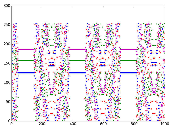
Red, green, blue and magenta are the four different sets of 8 bits each. It doesn’t look much like a sine wave, but that’s to be expected, having the FPGA signal order match order they are connected the ADC would have been astonishingly lucky.
There are patterns in the signal through. A 3kHz sine wave sampled at 1Msamples/second and with 1000 samples in the plot means that the signal should repeat three times in the capture, and it does.
The data mostly looks like random noise but it flattens out every now and then. And there are some things in the middle of the noise, that could be sine wave shaped if I squint a bit and wish really hard.
Positive or negative
After thinking a bit I realised that when I booted Linux some of the GPIOs changed which in turn switched the attenuation relays in the analog frontend (AFE) to a different range. This makes the signal swing higher and the flat parts is when the signal goes beyond the limits of the ADC and is clipped to all ones.
And after thinking a bit more I realised that the clipping was a good thing. Each differential signal consists of two wires with opposite polarity. When routing the wires it is sometimes easier to connect the positive pin from the transmitter to the negative pin on the receiver and vice versa. This makes the PCB layout simpler but means that the polarity of the signal will be inverted at the receiver. But since the signal is clipped and there should have been long stretches with all ones in the capture data, all bits that were zero in those stretches must be inverted.
Invert those signals in the decoder and plot the capture data again.
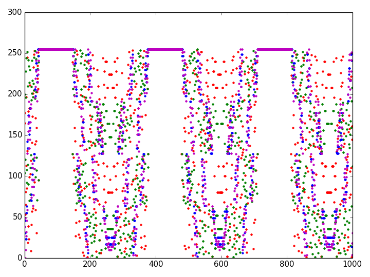
Now the flat regions are all ones and the regions in between actually show some signs of having sine waves in them.
The power of statistics
What can I do next? I had a feeling that the lower valued bits of each 8 bit set of signals will change more often than the higher valued ones, so why not collect some statistics.
Sort the signals by the number of transitions and group them four by four.
| Transitions | Signals |
|---|---|
| 6 | E13 F12 J14 K15 |
| 18 | F10 H13 H15 L14 |
| 42 | D11 G12 G14 M15 |
| 84 | C11 F15 J13 N14 |
| 173 | P15 B14 E15 J11 |
| 335 - 357 | K12 B15 M13 D14 |
| 358 - 368 | B10 R15 T14 C13 |
| 406 - 427 | L12 R14 C15 B12 |
A sine wave which repeats 3 times will change the highest valued bit twice for every repetition which means 2 * 3 = 6 transitions which matches the first line. The other lines are multiples of three all the way up to 173 which is one less than 58 * 3 = 174; the signal is probably a bit off center compared to the full range. The number of transitions for the lowest three bits varies so they might be mixed up and some of these transitions are probably just noise.
Rearrange the bits to match the table above and reanalyze the capture data:
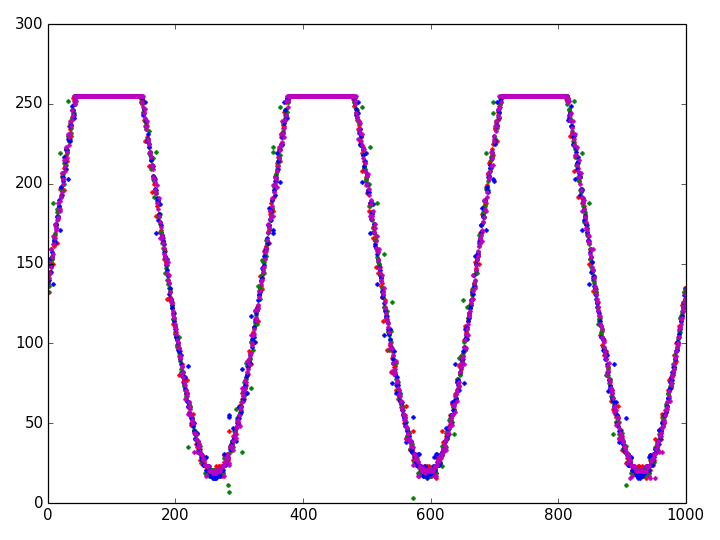
Whoa! That definitely looks like a clipped sine wave. There is a lot of noise but it’s starting to look decent.
Hmm, what next. Since all sets of bits contain similar data the ADC has to be in the mode where it interleaves all four sets for channel
- Let’s reboot the scope with the OWON firmware and turn on both channel 1 and channel 2 with the same source signal. Now two of the sets should be interleaved for channel 1 and the other two sets should be interleaved for channel 2. Back to Linux again and make a new capture:
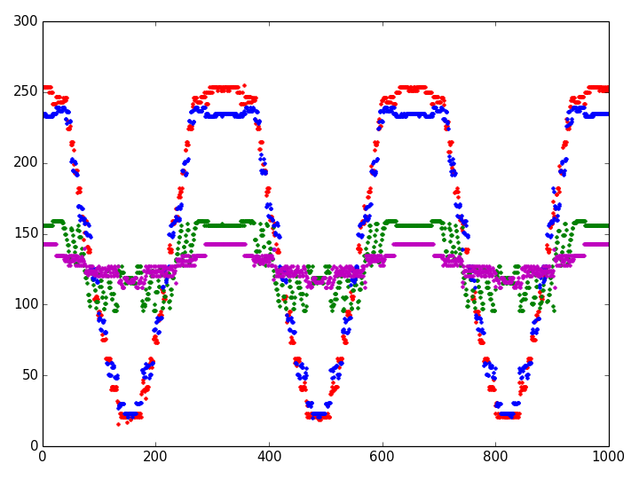
The bits for the two channels seem to be a bit mixed up, so let’s try the trick of finding parts of the signal that are clipped signal and swap around bits between sets until the first two sets are all ones.
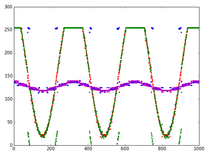
That looks a lot better, the red and green sets are for channel 1, the blue and magenta sets are for channel 2. There’s an obvious mix-up between the green and blue sets. Between samples 80 and 230 the value of the blue samples are 128 too high and the green samples are 128 too low. Swap the bits with value 128 between the sets.
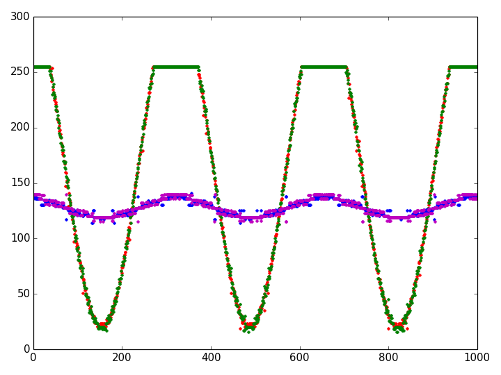
This is starting to look decent. There are still some artefacts down at the three lowest valued bits but it’s not too bad. I just ended up swapping the low valued bits around a bit randomly until the plots looked decent. This is that I finally ended up with:
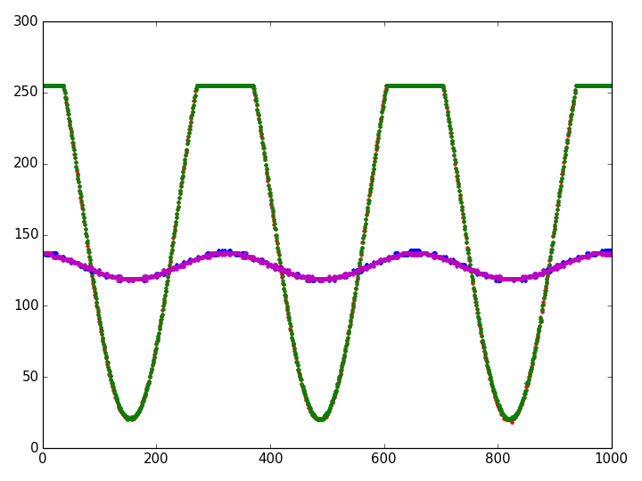
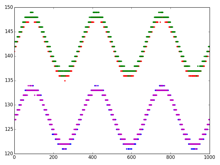
And if I increase the attenuation a bit it looks like this:
I think I’m good, each set looks decent now. I might still have messed up the order between the sets, what I think is set 1 of channel 1 might actually be set 2 from channel 1. I’ll have to play around a bit with higher frequency signals later and see if I can figure out if the order is correct or not.
But I can finally use the scope to capture signals, whee. My work is done for today.
Update: A new post is up.