More SDS7102 FPGA pins
This is a post in a series about me poking at the insides of my OWON SDS7012 oscilloscope. You might want to start reading at the beginning.
I’m sorry for being so quiet for the last few weeks, but I’ve had a bit much to do at work and also ended up going on a business trip to Boston. Sometimes work gets in the way of my hobby projects.
Anyway, in my last post I had just managed to program the FPGA in the scope with an image that counted edges on all the I/O-pins. This way I was able to figure out what some of the I/O pins were doing, for example one pin was toggling at 10MHz and is probably driven by the 10MHz crystal oscillator in the scope.
I like building tools
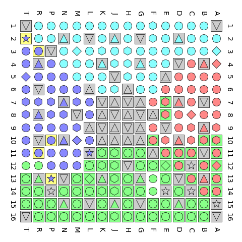
There are a lot of pins with different functions on the FPGA. Some of the pins are in different I/O banks which can have different I/O voltages and I/O standards. To make life easier for myself I copied the information from the Spartan-6 FPGA Packaging and Pinouts document (UG385) and wrote a small Python program which outputs a PNG image with a map of how the pins are used.
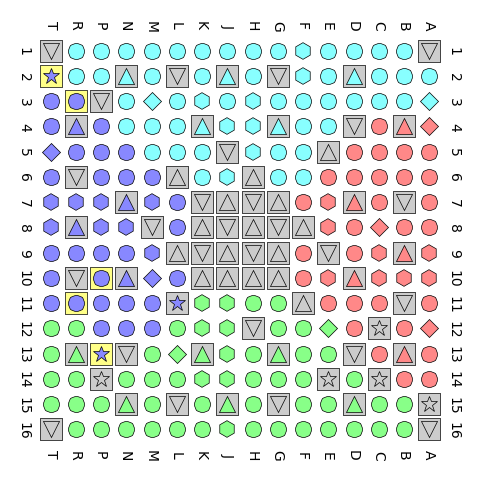
The shape of symbols show the function of the pin. A round symbol means that the pin is a normal I/O pin. A hexagonal symbol means that the pin can be a normal I/O pin or a clock input. A diamond is an I/O pin or a VREF pin which needed by some I/O standards. The other types of pins have dedicated functions and can not be used as I/O pins.
The color of the symbol shows what I/O bank it is in. The power supply pins for the internal logic in the FPGA and the ground pins do not belong to any I/O bank and are gray. The colored square around some pins indicates what function I believe the pin has. For example the yellow squares indicate that the pins are used for configuring the FPGA. The color of the symbol for those pinse is blue indicating that they use the I/O voltage from bank 2. Pins P10, R3 and T11 round and can be used as I/O pins after configuration; pins L13 and T2 are dedicated configuration pins and can not be used as I/O pins. L11 and N14 are not used for configuration on the scope and are gray. A15, C12, C14, and E14 are used for JTAG and I haven’t been able to find those signals anywhere, they are probably not connected to anything.
The SoC bus
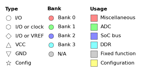
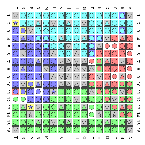
In my last post I had just discovered that a bunch of pins were toggling all the time. They are probably connected to the DDR memory bus of the SoC. I believe that this is the main way the SoC communicates with the FPGA, the FPGA simulates a DDR memory which is then read or written from the SoC. I just marked all those pins as the “SoC bus” pins in my tool and generated a new pin map.
As you can see, most of these pins are located in bank 2 but some of them are also located in bank 3. Bank 2 is physically closest to the SoC so it makes sense from a PCB layout standpoint too.
The I/O standard used for DDR2 memories is SSTL 1.8V which requires an external 0.9 reference voltage on VREF. I’ve found a resistive voltage divider on the PCB which is used to generate it.
Pins P7 and M7 are the differential 133MHz memory clock from the SoC.
I haven’t figured out the function of each individual pin in the SoC bus. I have few ideas on how to do it but haven’t had time to try them out yet.
The DDR bus
The FPGA has its own DDR memory. I’m hoping that the OWON hardware designers use the same pinout as Xilinx does in their MIG - Memory Interface Generator (UG388), so I added those pins to my pin map.
The DDR memory is located just above the FPGA so the physical PCB layout makes sense here too. Once again the I/O standard is SSTL 1.8V so the VREF pins are used for a 0.9V reference voltage.
So far so good, but I do have a bit of a problem here.
As you can see, I have marked eight of the pins in bank 3 as not used by the DDR controller. That is because those pins were toggling all the time and are most probably a part of the SoC bus. This should be OK most of the time, for example pin B1 is M3BA2 (Memory controller 3, bank address 2). Since the DDR2 memory chip only has two banks, only M3BA0 and M3BA1 are needed and M3BA2 is free. Pin F4 should be M3CKE (Clock Enable) which has a corresponding pin on the DDR memory but it’s probably possible to hardwire that pin on the DDR memory side to free up the pin on the FPGA side.
The big problem is that the Xilinx documentation clearly says that one of pins M4, M5, N4, or B3 should be used for RZQ calibration and must be left floating. Quoting Xilinx: “The RZQ pin is required and cannot be removed from the design”. But all these pins are connected to the SoC bus. I don’t have enough experience with the MIG to know how to make it work when a PCB designer ignores the Xilinx recommendations.
Except for this problem it should be fairly straightforward to use the Xilinx MIG and instantiate a memory controller on the FPGA.
The ADC bus
The last big bus connected to FPGA is the bus to the ADC. I realised that if I boot the scope normally and then use OpenOCD to perform a soft reset of the CPU and boot Linux, the ADC will still be running and most of the pins from the ADC will still be toggling.
The ADC signals are differential signals, and when I started looking at the frequencies each pin was toggling at it was quite clear that the frequencies came in pairs and that there were 32 of them. Well, that’s exactly what I’d expect since the ADC has 32 differential data outputs (2 channels with 2x8 bits each).
The ADC is physically located below the FPGA so that also makes sense.
This is all too easy.
The frequency on the differential pair at E7 and E8 that was toggling even with the ADC off was most probably the sampling clock output from the ADC (DCLK+/DCLK-). I rebooted the scope, changed the horizontal resolution and booted back to Linux and my FPGA test image again and the frequency had changed. I’m pretty convinced that it is the sampling clock.
When I later poked at some pins of the ADC I also managed to make pins F13 and F14 toggle. I’m not sure exactly what they do. They might be the overrange and CalRun outputs from the ADC.
I don’t know exactly which differential pairs on the FPGA map to the data outputs from the ADC but that shouldn’t be too hard to figure out. If I can get the analog frontend (AFE) to work it should be possible to adjust the gain so that only the lowest bit of the data outputs toggle to begin with. If I then increase the gain higher data bits should start toggling and this way it should be possible to figure out which pair does what in a smarter way than just brute forcing all possible combinations.
All the rest
With all the big mapped and out of the way I could start looking at all the remaining pins. I used the same method as for finding SoC pins, configure a pull up or pull down on the pins and then force interesting pins on the PCB high or low using a 330 Ohm resistor to VCC or GND and see which pins are toggled on the FPGA.
The first thing I probed was the I2C bus on the AT88SC crypto memory. Pin C4 on the FPGA turned out to be connected to the SCL pin and B6 to the SDA pin. Now when I think of it that actually makes sense, if OWON somehow puts the serial number and the license key in the Spartan 6 FPGA they can also put the license check inside the FPGA making it much harder to circumvent. Smart.
Pin C10 is probably the 10MHz reference clock from the crystal oscillator on the scope.
Pins A5, B5, B8, C6, and D6 were connected to the front panel connector. I’ll have to figure out what they do later.
Pin A7 is the chip select (CS) pin on the LMH6518 for channel 1.
Pin C8 is the chip select (CS) pin on the LMH6518 for channel 2.
Pin F7 is the load (LD) pin on the Rohm DAC. Update: I had made a mistake in my pin diagram and used to think E6 was connected to the DAC, this was wrong, F7 is the correect pin.
Update: I have later found out that pin A8 is connected to the TI DAC.
Pin C7 is the latch enable (LE) pin on the ADF4360-7 clock generator.
Pin F9 is probably the chip select (CS) pin on the ADC.
Pin D9 is a serial clock and pin D8 is serial data. These pins are connected to the clock and data pins of all of the above chips.
I also noticed that when I ran the scope off the AC line instead of from battery pin A4 would toggle at 50Hz. Hmm. Let’s check the specifications, yes, the scope can be triggered of the AC line. I guess that’s it then.
Pin D5 toggles at 1kHz if I connect a scope probe from channel 1 to a 1kHz probe compensation signal. I’d guess this is the output from the trigger circuit for channel 1 of the scope. I haven’t found the trigger for channel 2 or the external trigger yet but that should be easy to figure out once I know how to configure the AFE. Two more pins ought to be connected to the video trigger ICs. I’m not sure where I’ll find a composite video source today, composite video is just so 20th century you know. I might just have to dig out my old Amiga 1000 from the basement and hope that it still is working.
I had to work a bit harder to find the pins for the probe compensation output on the front and external trigger output on the back. They are driven via some circuitry so I had to look at the PCB traces and take a guess where the inputs would be. Not too hard, but needed a bit more thought than just forcing input pins on an IC low.
T11 controls the probe compensation output and is pulled high via resistor R125 on the PCB. Also note that T11 is the M0 input which together with M1 are used to select the configuration mode for the FPGA at power on. M1 is pin N11 of the FPGA and is pulled high via resistor R124 on the PCB. Both of these pins are sampled by the FPGA when it is powered on, so they must not be driven low by anything else in the scope. Since T11/M0 is an output it should be safe, it’s never driven by anything but the FPGA, and I have not found anything connected to N11/M1 it should also be safe.
E10 controls the external trigger output on the back of the scope.
R12 always toggles at something like 17kHz. I have no idea what it does.
Final pin map
With all these pins filled in, here’s the pin map.
As you can see there are a dozen I/O pins left on the FPGA that I haven’t found yet. Some will turn out to be triggers. Some may be ADC signals. Some may be unused.
Other than that I actually think that I have mapped out just about every connection in the scope. I know how the SoC is connected to all the SoC peripherals and some of the components in the AFE. I mostly know how the FPGA is connected to the SoC, the DDR memory, the ADC and the other parts like the clock generator, DAC and remaining components in the AFE.
The FPGA-SoC bus is going to be tricky to get to run. It’s a fast bus and any mistakes in the signaling from the FPGA will corrupt memory for the SoC and crash the scope. It’s going to be painful to test and debug. The DDR memory controller in the FPGA does not seem to follow the Xilinx recommendations and I’m not sure how to solve that either.
It shouldn’t be too hard to create an image for the FPGA that can set up the clock generator and AFE and then record data from the ADC into internal block RAM on the FPGA and then slowly transferred to the SoC using the three I/O pins I’ve been using to communicate with the FPGA so far. I’ll probably start there. There will be lots of small things that have to be in place for this to work setting up the DAC, clock generator, ADC, triggers and all other parts in the AFE. Probably nothing that’s very hard, just time consuming and since I’m fairly new at hardware description languages (HDLs) it’ll take a lot of time.
But that’s what hobby projects are for, aren’t they? It’s something to do for fun when one has a bit of time left over and with a bit of luck I’ll learn something on the way.
I’ll probably be quiet for some time while I’m trying to learn more about MyHDL. If anyone has a SDS7102 scope (or some of the other scopes in the same series, they ought to be fairly similar) and would like to help out, or just is interested, I could clean up the things I’ve done so far and upload everything to a GitHub repository. If I’m too slow at doing this, send me a mail and remind me.
Until next time.
Update: I lied. I had enough material for one more post left in my notes.