SDS7102 OS Disassembly
This is a post in a series about me poking at the insides of my OWON SDS7012 oscilloscope. You might want to start reading at the beginning.
In the last post I had just managed to extract some files from the dump of the NAND flash I had made. Most importantly I had an “os” file which probably contained the scope operating system and an “fp” file with the FPGA bitstream.
Where to start
Disassembling binary code is tedious and often boring work. Going through a 3MByte large binary such as the “os” file would take ages so I decided to cheat a little.
What I was mostly interested in was code that touched the hardware, that really means the GPIO pins. Most of the time when the code accesses GPIO register it loads the base address for the whole bank of GPIO registers into a CPU register and then uses that CPU register with an offset to access the other GPIO registers.
The base address for the GPIO registers is 0x56000000. And the binary code for an ARM instruction loading this value into a register is 0xe3a0?456. The ? is the CPU register number and the 56 at the end is the highest eight bits of the address. Finding instructions as this is trivial, show a hexdump of the file, pipe it to less and use the “/” command in less to search for the bytes making up that instruction:
$ hd "os" | less
/56 .4 a0 e3
I then used Medusa to disassemble the code near these addresses and walk through what the code was doing. Tedious, but not quite as tedious as trying to disassemble everything.
Finding something
As an example, I found a couple of wrapper functions that controlled the GPB4 and GPB9 pins.
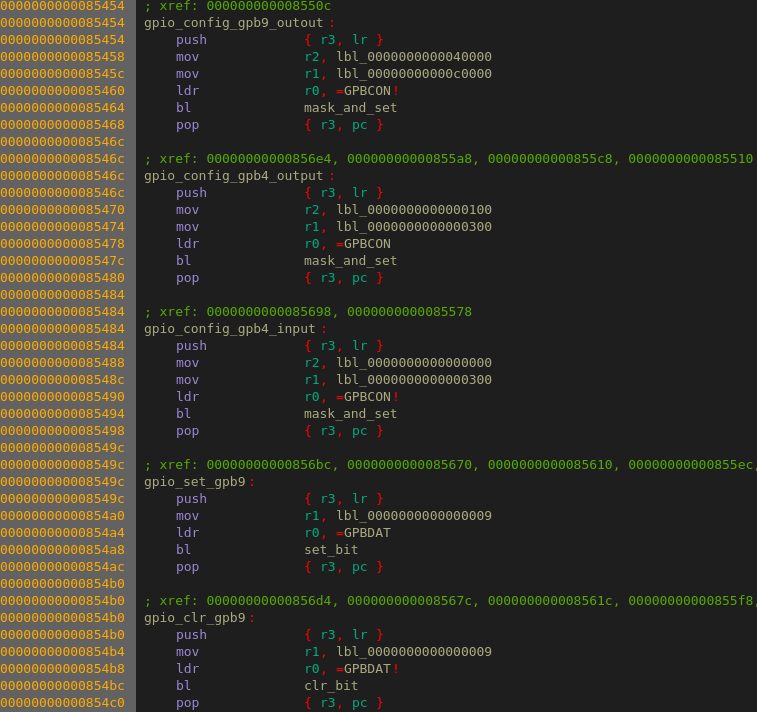
Not that useful in themselves, but I gave the functions descriptive names and continued with the disassembly. Just below in the disassembly I found the following code which used the wrapper functions:
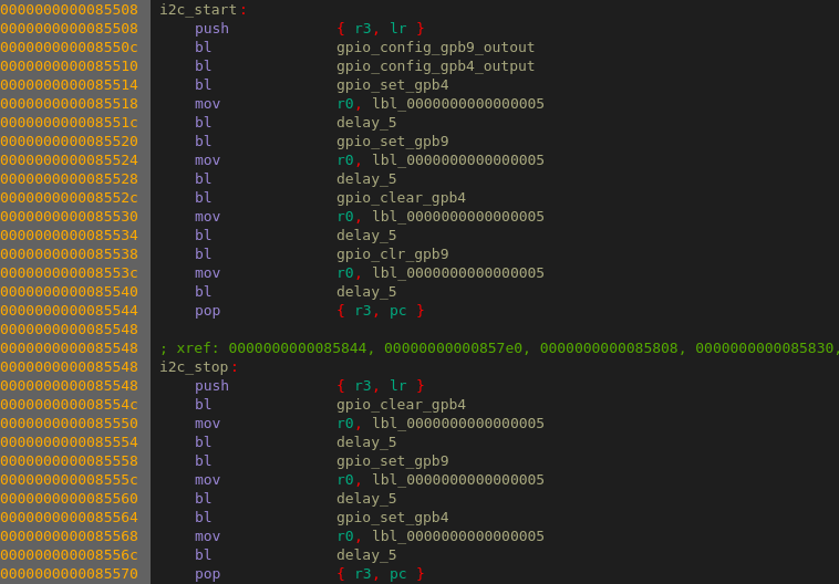
As you see from the names I’ve given the functions I have already figured out that these pins are used for an I2C bus. The first function “i2c_start” configures GPB4 and GPB9 as outputs, drives both high and then drives GPB4 low before driving GBP9 low. The second function drives GPB4 low, GPB9 high and finally GPB4 high.
Here’s an image from an I2C tutorial showing some of the signaling on an I2C bus:
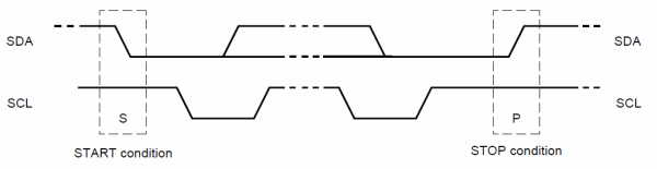
If GPB4 is SDA and GBP9 is SCL the code perfectly matches the I2C START and STOP conditions. More functions further down in the disassembly implemented I2C Write and I2C Read operations, but the functions are a bit too long so I won’t show them here.
Linux does it with tables
Time to test this in Linux. Linux already has an I2C driver “i2c-gpio” which can use any two GPIO pins as an I2C bus. I added the following to the machine definition “mach-smdk2410.c” that I was using for my Linux port to the scope:
static struct i2c_gpio_platform_data sds7102_i2c_pdata = {
    .sda_pin        = S3C2410_GPB(4),
    .scl_pin        = S3C2410_GPB(9),
};

static struct platform_device sds7102_i2c_chrontel = {
    .name           = "i2c-gpio",
    .id             = 1,
    .dev            = {
	    .platform_data = &sds7102_i2c_pdata,
    },
};

static struct platform_device *smdk2416_devices[] __initdata = {
    ...
    &sds7102_i2c
};
Boot up the scope, load the driver and use the tool “i2cdetect” from the I2C Tools package to scan the I2C bus for something interesting:
# i2cdetect -y 1
    0  1  2  3  4  5  6  7  8  9  a  b  c  d  e  f
00:          -- -- -- -- -- -- -- -- -- -- -- -- --
10: -- -- -- -- -- -- -- -- -- -- -- -- -- -- -- --
20: -- -- -- -- -- -- -- -- -- -- -- -- -- -- -- --
30: -- -- -- -- -- -- -- -- -- -- -- -- -- -- -- --
40: -- -- -- -- -- -- -- -- -- -- -- -- -- -- -- --
50: -- -- -- -- -- -- -- -- -- -- -- -- -- -- -- --
60: -- -- -- -- -- -- -- -- -- -- -- -- -- -- -- --
70: -- -- -- -- -- -- 76 --
There seems to be an I2C device at address 0x76 on the bus. I went through the data sheets I had collected when I had the scope open and tried to locate interesting components. I hadn’t been able to find a data sheet for the Chrontel CH7026 VGA chip but I did find a data sheet for the CH7028 which seems to be a close relative to it. The Chrontel chip uses I2C for communications and is at address 0x76. Bingo!
The register format used in the Chrontel is supported by the “i2cdump” tool so why not dump the register contents:
# i2cdump -y 1 0x76 b 0
     0  1  2  3  4  5  6  7  8  9  a  b  c  d  e  f    0123456789abcdef
00: 54 00 03 00 01 08 73 1f 00 00 00 00 00 00 e0 09    T.?.??s?......??
10: 40 ad 00 40 10 08 f0 5f 00 20 03 35 46 b4 00 40    @?.@???_. ?5F?.@
20: 10 11 e0 0d 00 20 03 08 01 40 00 01 f0 00 40 47    ????. ???@.??.@G
30: 40 80 74 08 00 08 00 40 00 40 00 40 00 9c 21 00    @?t?.?.@.@.@.?!.
40: 00 b2 00 00 00 00 00 00 00 10 6f 7a 5a 08 00 00    .?.......?ozZ?..
50: 00 40 09 1c 00 e4 80 00 00 00 00 00 00 40 08 00    .@??.??......@?.
60: 00 00 00 00 00 00 00 00 00 5a 00 40 00 00 00 00    .........Z.@....
70: 15 15 10 10 89 a2 0c 43 22 18 18 00 00 60 00 00    ???????C"??..`..
80: 54 00 03 00 01 08 73 1f 00 00 00 00 00 00 e0 09    T.?.??s?......??
90: 40 ad 00 40 10 08 f0 5f 00 20 03 35 46 b4 00 40    @?.@???_. ?5F?.@
a0: 10 11 e0 0d 00 20 03 08 01 40 00 01 f0 00 40 47    ????. ???@.??.@G
b0: 40 80 74 08 00 08 00 40 00 40 00 40 00 9c 21 00    @?t?.?.@.@.@.?!.
c0: 00 b2 00 00 00 00 00 00 00 10 6f 7a 5a 08 00 00    .?.......?ozZ?..
d0: 00 40 09 1c 00 e4 80 00 00 00 00 00 00 40 08 00    .@??.??......@?.
e0: 00 00 00 00 00 00 00 00 00 5a 00 40 00 00 00 00    .........Z.@....
f0: 15 15 10 10 89 a2 0c 43 22 18 18 00 00 60 00 00    ???????C"??..`..
Register 0 is the device ID and is supposed to be 0x54. Well, that’s also correct. Good. Not that I’m too interested in VGA at this stage but if I wanted to enable the VGA port there’s a possibility that it might work.
Note to self: Try connecting the scope to a monitor and then rebooting into Linux without resetting the Chrontel chip. If I’m lucky I should get an image on the monitor and should be able to dump a working Chrontel configuration to a file.
That’s two more pins out of a couple of hundred that I’ve found the function for. One step at at time does it.
Programming the FPGA
Another thing I found was some code that loaded the “fp” file and then did this which I recognized as Xilinx FPGA related operations:
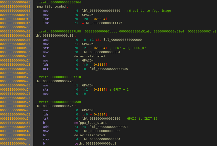
translated into pseudo-C, with my comments, it does something like this:
/* Reset FPGA by driving PROG_B low for a short while */
gpio_set_value(GPK7, 0); /* drive PROG_B low */
delay_calibrated(100);
gpio_set_value(GPK7, 1); /* drive PROG_B high */

/* Wait for INIT_B to go high which indicates that the FPGA is ready */
for (i = 0; i < 100; i++) {
    if (gpio_get_value(GPK13)) /* read INIT_B */
    break;
    delay_calibrated(50);
}
if (i == 100) {
     /* error handling */
}
the code then then looped through each byte of the file and did this:
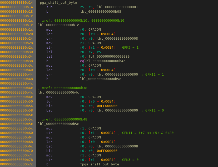
Translated into pseudo-C:
/* Shift 8 bits of data into the FPGA */
uint8_t b = fpga_data[i];
for (j = 0; j < 8; j++) {
gpio_set_value(GPK3, 1); /* drive CCLK high */
if ((b << j) & 0x80)
    gpio_set_value(GPK11, 1); /* set DIN to 1 */
else
    gpio_set_value(GPK11, 0); /* set DIN to 1 */
gpio_set_value(GPK3, 0); /* drive CCLK low */
}
This looks very much like shifting the FPGA data one bit at a time.
When it had gone through all bytes from the FPGA file it did this:
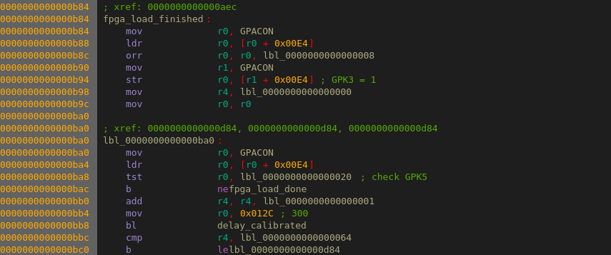
gpio_set_value(GPK3, 1); /* one final CCLK edge */

/* wait for DONE to go high when the bitstream has loaded */
for (i = 0; i < 100; i++) {
    if (gpio_get_value(GPK5)) /* read DONE pin */
    break;
    delay_calibrated(300);
}
if (i == 100) {
     /* error handling */
}
This is algorithm is almost straight out of the Spartan-6 FPGA Configuration User Guide (UG380) describing how to program a bitstream into a Xilinx FPGA using Slave Serial Mode.
Simon Says
I have written a couple of Xilinx FPGA loaders before but couldn’t find any of them so I quickly wrote a new Linux device driver. The driver creates a device called “/dev/fpga” which does almost exactly the same thing as the code from the disassembly above.
When the “/dev/fpga” device is opened it pulls PROG_B/GPK7 low for a short time and waits for INIT_B/GPK13 to go high. Any data written to the device will be shifted out using DIN/GPK11 as the data pin and CCLK/GPK3 as the clock. When the device is closed it waits for the DONE/GPK5 pin to go high.
Loading an FPGA image from Linux is as easy as writing a file to the device:
# cat fp >/dev/fpga
PROG_B <- 0  (this happens when the device is opened)
INIT_B -> 0
PROG_B <- 1
INIT_B -> 1
DONE_B -> 0
...          (data is written here)
DONE_B -> 1  (this happens when the device is closed)
This loaded the original FPGA image from the “fp” file in the flash dump. I also tried building my own little FPGA image which just toggled the INIT_B line every second and from Linux I could then see the GPK13 change.
Five more pins down, much too many left to go.
More, more, more!
I find some other pins that made relays inside the scope click. For example changing GPA1 makes a relay click and in the disassembly both GPA12 and GPA15 are usually changed at the same time. They probably have something to do with each other; if GPA1 turns out to control one of the relays in the analog front end for channel 1, GPA12 and GPA15 probably control something else for the same channel such as the AC/DC solid state relay or the analog mux in each frontend.
GPB3 controls the brightness of the display, if it’s off the screen dims a bit, if it’s on the screen becomes brighter. Since GPB3 can also be configured as a timer output it should be possible to change the display brightness in multiple steps between dimmest and brightest.
I found out that GPF3 turns on or off the Run/Stop LED. I haven’t figured out how to control the color yet.
GPF2 is read in close proximity to the code that controls the USB device port. If I read the disassembly correctly GPF2 ought to be a VBUS detect input, just as on the SMDK2416, but I haven’t been able to make it change when I tried connecting or disconnecting the USB cable. This needs more testing.
I found out that GPE11, GPE12 and GPE13 are used for the SPI bus the ethernet chip, that GPL13 is used as the chip select, and that GPF1 is the interrupt from the chip. I already knew that though.
There are other things that don’t make sense. There’s code that touches GPJ2 and GPJ3. But there is no GPJ port on the S3C2416. There are no such pins and no documentation for the registers. There is one line in the documentation which shows the addresses for the GPJ port, something that Samsung probably forgot when they wrote the manual and copy pasted from some earlier chip’s documentation. It still doesn’t make sense for the firmware to touch those registers.
There are a lot of other pins that the firmware touches that I don’t know what they do yet, but is on my list of things to try later.
Summary
Being lazy pays off. By searching for an instruction that references the GPIO registers and only disassembling code close to it didn’t take that long to find a lot of interesting things to try. I can now talk to and program the FPGA, how to talk to the Chrontel VGA controller and have a few more leads on what some other pins do.
I’ll try to write some Verilog code for the FPGA and see if I can discover anything that way, but I’m afraid that I’ll have to crack the scope open again pretty soon and start probing pins on the PCB to find out more.
Until next time.