Reverse Engineering, Part 2, Schematics
In my last post I described how I wanted to reverse engineer a RFID card reader. Read that post first if you haven’t.
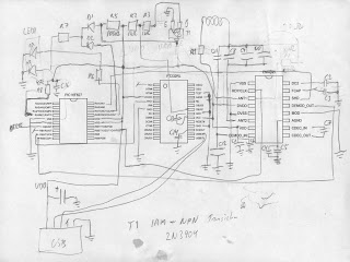
After identifying all the components on the board, the next step is to figure out how they are connected together. Since I had access to the data sheets for all the big ICs I threw together an image in OpenOffice Draw that i printed out so that I had something to make notes on, and this is the end result (click on the image for a larger version).
I then brought out my old trusty multimeter and switched it to the mode where it will beep if there is a connection between the probes, and started probing the board to find all the connections.
I usually start out by following the ground traces, it’s fairly easy, just put one probe on a known ground pad such as the housing of the USB connector and then use the other probe on just about everything else on the board. One reason for starting with the ground is that many small components are connected to it. For example, decoupling capacitors are connected to both ground and the voltage supply, pull up or pull down resistors are connected to either ground or the voltage supply, and in this circuit a couple of pins on the LEDs and on the transistor are also connected to ground. After that it’s a lot of boring work, systematically trying one pin after another with all other pins until all connections have been found.
This is a fairly easy board to reverse engineer since all the component pins are visible. For denser boards with BGA packages, many pins are hidden under the components. In those cases one has to guess or become more creative, for example by using an oscilloscope to measure the signals on the pin and try to figure out what pin it is by what the oscilloscope shows. But there is usually a lot of guesswork and intuition involved in this process. A bit of knowledge about the components, is a good idea since it means that one can make smarter guesses.
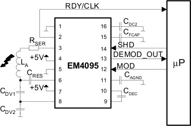
For example, it turns out that the reference schematics for the EM4095 almost perfectly matches my draft. The only differences are that some capacitors from the reference schematics are constructed out multiple capacitors in parallel on the actual board, and that the reader is in read/only mode: the MOD pin is grounded instead of connected to the microcontroller.

EM4095 - figure 8 - Read/Write mode (High Q factor antenna)
One thing that fooled me for a while here is that the resistance over the antenna is only 30 Ohm, and the resistor in series with the antenna is only 8.2 Ohm. For such small resistances my multimeter will beep and signal a connection, so for a while my draft had quite a lot of components connected together that really weren’t. When I realised what I had done I had to start over again with all those components and this time actually measure the resistance to get the correct results.
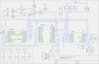
I then used the gschem (schematic capture) application from the gEDA project to produce a cleaned up version of the schematics.
So the RFID part is almost the reference design straight out of the EM4095 data sheet, the PIC decodes the DEMOD_OUT signal and outputs some data on it’s UART which is then transmitted over USB to the host PC by the FTDI controller. The VPP pin on the PIC is connected to VDD through a resistor which I believe is the recommended way to make the PIC in circuit programmable, so it ought to be possible to replace the firmware in the PIC.
The MOD pin is grounded, and the TX output from the FTDI controller is not connected to the RXD input on the PIC so it’s a pure read/only card reader, it can not write anything to a writable RFID tag. Yet…
So basically now I know all there is to know about this board and how it works. I have no idea what kind of firmware there is inside the PIC but since I know how the board works and have the data sheets for all the components it should be trivial to write a new firmware for the PIC.

